Rotary positioning device for semiconductor device processing

A positioning device, semiconductor technology, applied in semiconductor/solid-state device manufacturing, electrical components, circuits, etc., can solve the problems of increasing manufacturing costs, achieve self-locking function, and ensure the effect of rising stability

Active Publication Date: 2019-12-06
青岛融合装备科技有限公司
View PDF5 Cites 0 Cited by
  • Summary
  • Abstract
  • Description
  • Claims
  • Application Information

AI Technical Summary

Problems solved by technology

[0003] In the prior art, the production and processing requirements for semiconductor chips are very strict; in order to meet the huge demand in the existing market, the mass production equipment of the factory is indispensable, but due to the high precision of semiconductor chip production, so the processing equipment The work accuracy requirements are also striving for perfection. Therefore, in order not to cause excessive process costs, the timely elimination of defective products in the manufacturing process has also become the top priority. However, it is difficult for existing equipment to meet these series of work requirements, which leads to manufacturing Manufacturers need to pay more manpower to meet the requirements of the manufacturing process, which greatly increases the manufacturing cost; therefore, a new type of rotary positioning device for semiconductor device processing with high precision and mass production inspection is needed

Method used


Image

  • Rotary positioning device for semiconductor device processing
  • Rotary positioning device for semiconductor device processing
  • Rotary positioning device for semiconductor device processing

Examples


Embodiment

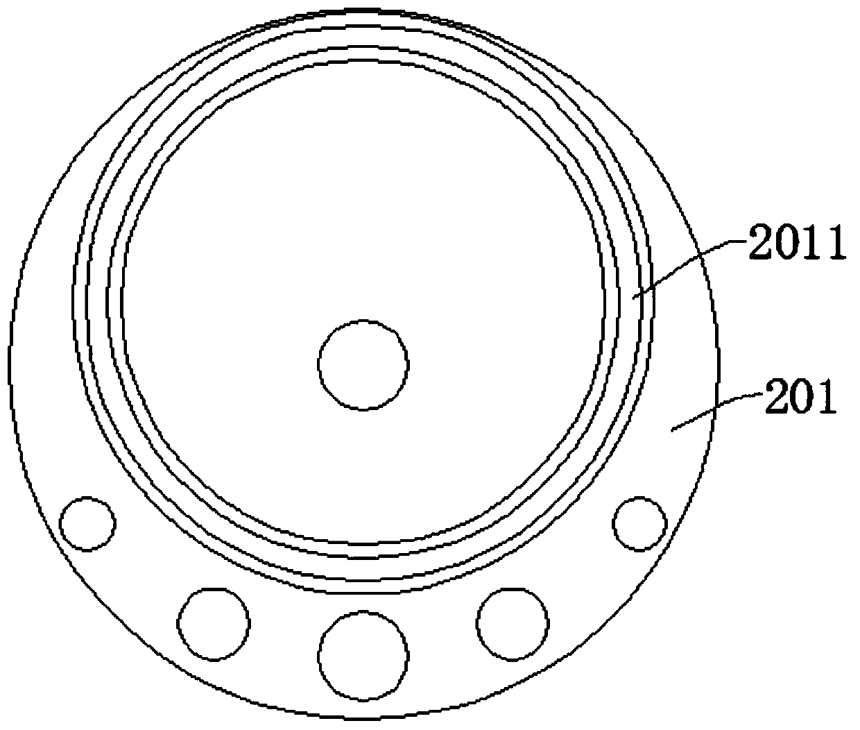
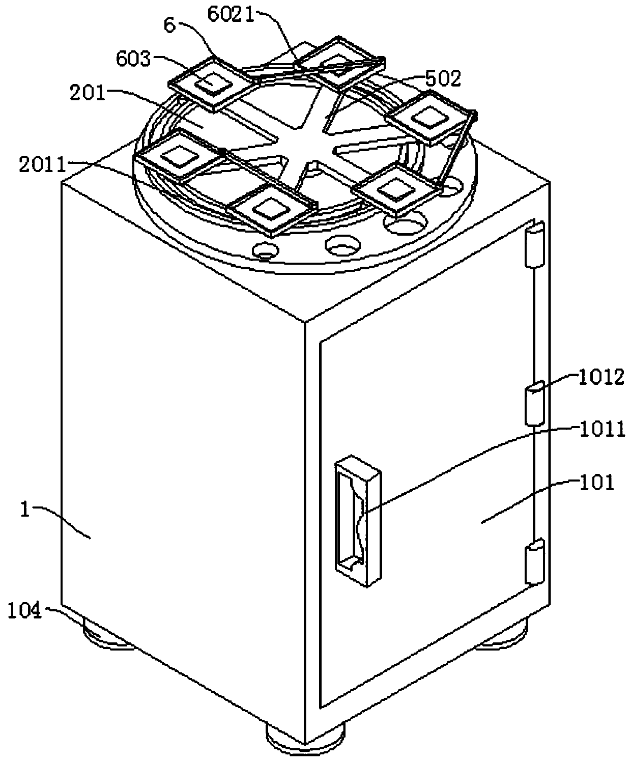
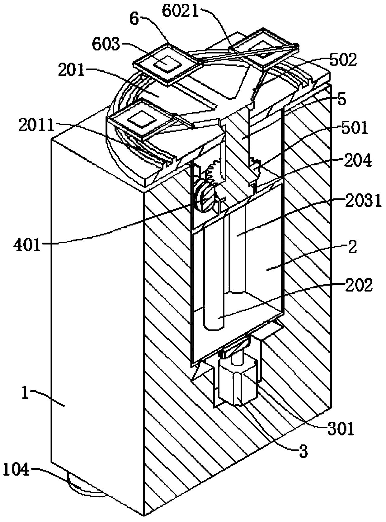
[0033] refer to Figure 1-8, a rotary positioning device for semiconductor device processing, including a mounting box 1, a first groove 102 is opened in the mounting box 1, a mounting table 2 is slidably connected to the first groove 102, and a turntable 201 is connected to the top of the mounting table 2 and It is integrally formed with the mounting table 2, and the turntable 201 is provided with an annular groove 2011, and a slide block 605 is slidably connected in the annular groove 2011, and a working frame 5 is connected in rotation in the mounting table 2, and a worm wheel 501 is connected to the working frame 5 and is connected with the working The frame 5 is integrally formed, the installation platform 2 is fixedly connected with the second motor 4, the output end of the second motor 4 is connected with the worm 401, the worm 401 is meshed with the worm wheel 501, and the working frame 5 extends through the turntable 201 to the top and is connected with a bracket 502,...


PUM


Abstract

The invention discloses a rotary positioning device for semiconductor device processing, and belongs to the technical field of semiconductor manufacturing. The rotary positioning device for semiconductor device processing comprises a mounting box which is internally provided with a first groove. A mounting table is slidably connected in the first groove. A rotating table is connected at the top ofthe mounting table. A ring groove is arranged in the rotating table. A slide block is slidably connected in the ring groove. A working frame is rotatably connected in the mounting table. A worm wheelis connected on the working frame. A second motor is fixedly connected in the mounting table. The output end of the second motor is connected with a worm rod. The worm rod is engaged with the worm wheel. The working frame penetrates through the rotating table to extend to the top and is connected with a bracket. A tray is rotatably connected on the bracket. A first rotating shaft is fixedly connected on the bottom of the tray. The first rotating shaft is rotationally connected with a slide block through a first connecting rod. A second rotating shaft is connected on the top of the tray. A second connecting rod is rotationally connected on the second rotating shaft. A workbench is fixedly connected on the tray. The rotary positioning device for semiconductor device processing has compact structure and accurate positioning and can perform comparative processing.

Description

technical field [0001] The invention relates to the technical field of semiconductor manufacturing, in particular to a rotary positioning device for semiconductor device processing. Background technique [0002] Semiconductors refer to materials whose electrical conductivity is between conductors and insulators at room temperature; semiconductors are widely used in consumer electronics, communication systems, medical instruments and other fields. No matter from the perspective of technology or economic development, the importance of semiconductors is huge. It is very huge; and the most common use of semiconductors is to make semiconductor chips. Semiconductor chips are etched and wired on semiconductor sheets to make semiconductor devices that can achieve certain functions. For example, diodes are made of semiconductors. Devices, the core units of electronic products commonly used in life, such as computers, mobile phones or digital recorders, are closely related to semicond...

Claims


Application Information

Patent Timeline
Patent Type & Authority Applications(China)
IPC IPC(8): H01L21/68
CPCH01L21/68
Inventor 王华珍
Owner 青岛融合装备科技有限公司
Why Eureka
Try Eureka