Miniature multilayer ceramic band-pass filter
A band-pass filter, multilayer ceramic technology, applied in multi-terminal pair networks, impedance networks, electrical components, etc., can solve problems such as negative effects on device performance, and achieve the effect of low insertion loss, length and width reduction
- Summary
- Abstract
- Description
- Claims
- Application Information
AI Technical Summary
Problems solved by technology
Method used
Image
Examples
Embodiment 1
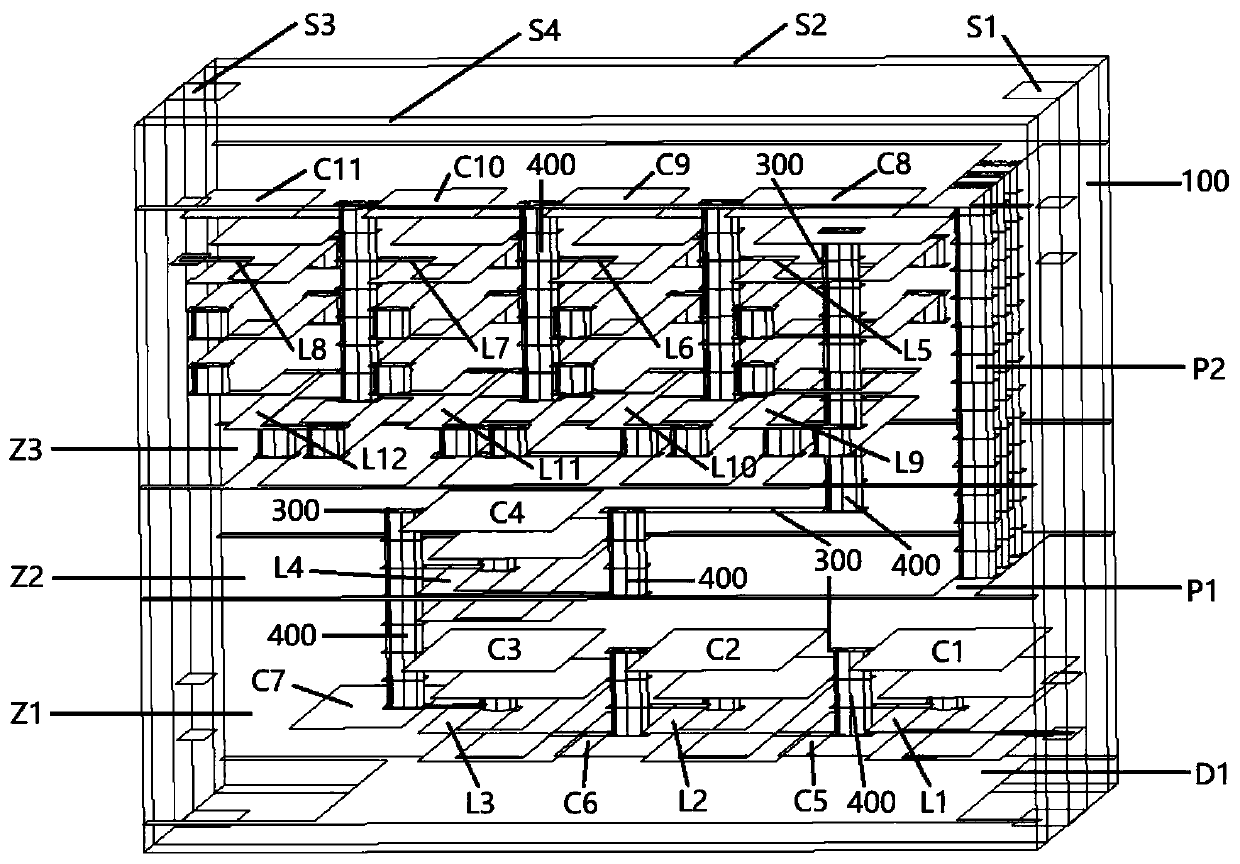
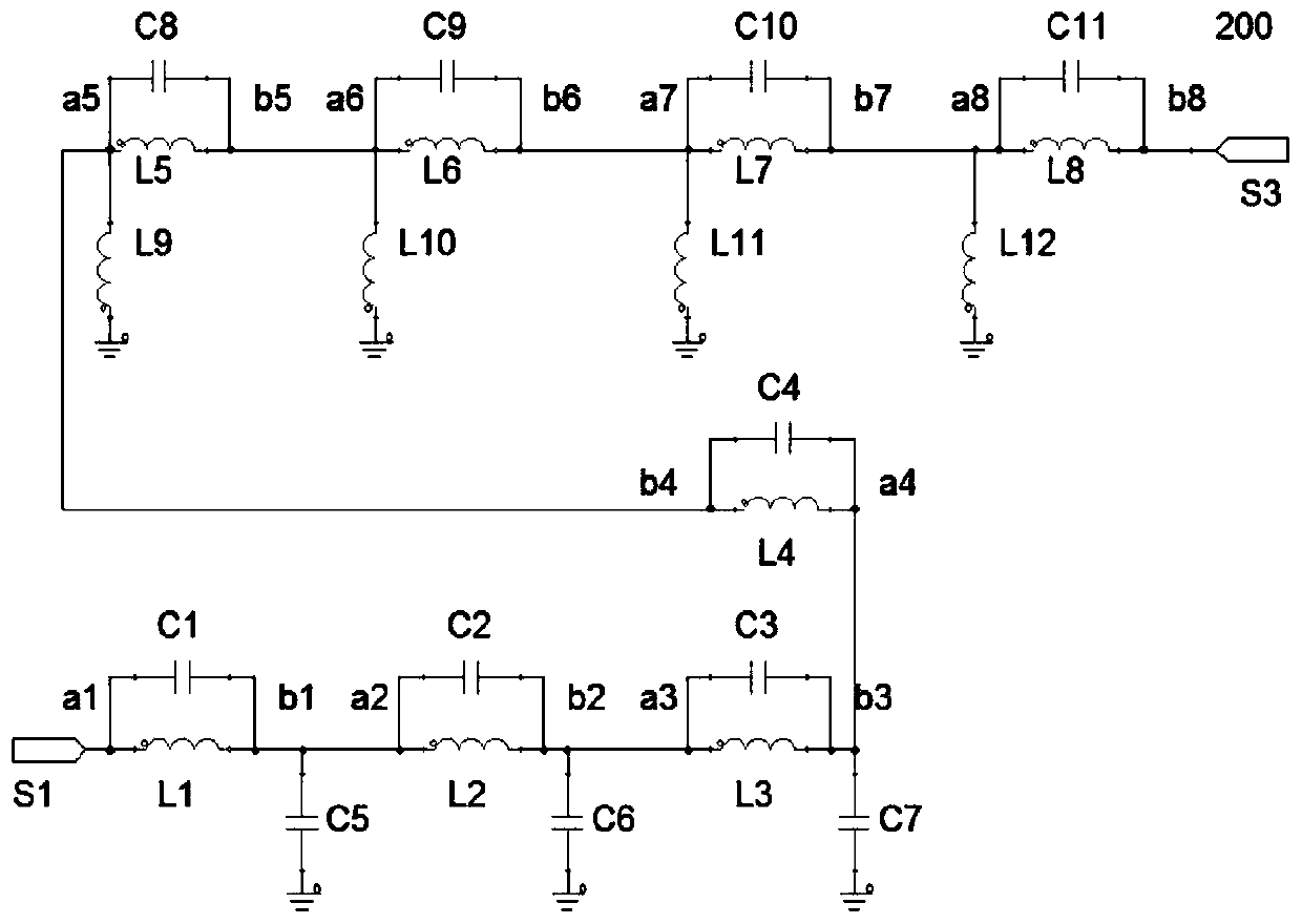
[0034] combine Figure 1 to Figure 3As shown, the miniature multilayer ceramic bandpass filter of this embodiment includes a central laminated body 100 and a filter circuit 200 disposed in the central laminated body. unit, each carrying unit is composed of multi-layer dielectric substrates stacked from top to bottom, adjacent dielectric substrates are connected to each other through conduction strips 300 and via holes 400, and the surface of the central laminate 100 is provided with a first input The output terminal S1 and the second input and output terminal S3; also include two grounding side plates S2 and S4, and the two grounding side plates S2 and S4 are located on the sides of the central laminated body 100 .
[0035] In this embodiment, in the filter circuit, the number of the first transmission zero structure and the second transmission zero structure are four respectively; and the first transmission zero structure is a parallel structure of an inductor L and a capacit...
Embodiment 2
[0047] Such as Figure 4 to Figure 7 As shown, compared with Embodiment 1, this embodiment is only different in that: the first transmission zero point structure at the end, like the other three first transmission zero point structures at the front end, adopts a common connection structure, that is, sequential connection Structural implementation:
[0048] That is, the parallel structure of L4 and C4, its input end face a4 is the same as the input and output ends a1, a2, and a3 of the other three first transmission zero point structures, and they are all located on the same side as the first input and output end S1, that is, they are all located at The left side of the parallel connection structure of L4 and C4, and the output end surface b4 is located on the left and right sides of the parallel connection structure of L4 and C4 with the first input and output terminal S1. Compared with the folding structure, this sequential structure is not compact enough. When the parallel ...
PUM
 Abstract
Description
Claims
Application Information
 - R&D
- Intellectual Property
- Life Sciences
- Materials
- Tech Scout
- Unparalleled Data Quality
- Higher Quality Content
- 60% Fewer Hallucinations
Browse by: Latest US Patents, China's latest patents, Technical Efficacy Thesaurus, Application Domain, Technology Topic, Popular Technical Reports.
© 2025 PatSnap. All rights reserved.Legal|Privacy policy|Modern Slavery Act Transparency Statement|Sitemap|About US| Contact US: help@patsnap.com


