Non-destructive absorption circuit of active PFC circuit

A non-destructive absorption and circuit technology, applied in the direction of high-efficiency power electronic conversion, electrical components, output power conversion devices, etc., can solve the problems of reducing the output efficiency and loss of the whole machine, so as to improve the output efficiency of the whole machine, strong reliability, The circuit achieves simple effects

Inactive Publication Date: 2019-09-06
APM TECH DONGGUAN
View PDF6 Cites 0 Cited by
  • Summary
  • Abstract
  • Description
  • Claims
  • Application Information

AI Technical Summary

Problems solved by technology

[0002] At present, under the condition that switching power supply has higher and higher requirements on power factor PF, the PFC circuit of switching power supply needs to use active PFC circuit to achieve higher PF value, and the power switch tube of active PFC circuit works at high frequency On -Off state of fast cycle switching, DV / DT and DI / DT are changing rapidly, so for EMI, the PFC power switch is not only the main interference source of electric field coupling, but also the main interference source of magnetic field coupling, plus the PCB on the The parasitic inductance will generate a peak voltage between the D pole and the S pole when the power switch tube is turned off. The larger the parasitic inductance will be, the higher the peak voltage will be. The traditional method is to connect the D pole and the S pole of the power switch tube in parallel. A capacitor absorbs the peak voltage caused by the parasitic inductance of the PCB when the power switch tube is turned off, but this method will cause loss and reduce the output efficiency of the whole machine, and the EMI interference will not achieve the best effect

Method used


Image

  • Non-destructive absorption circuit of active PFC circuit

Examples


Embodiment Construction

[0011] In order to facilitate the understanding of those skilled in the art, the present invention will be further described below in conjunction with the embodiments and accompanying drawings, and the contents mentioned in the embodiments are not intended to limit the present invention. The present invention will be described in detail below in conjunction with the accompanying drawings.

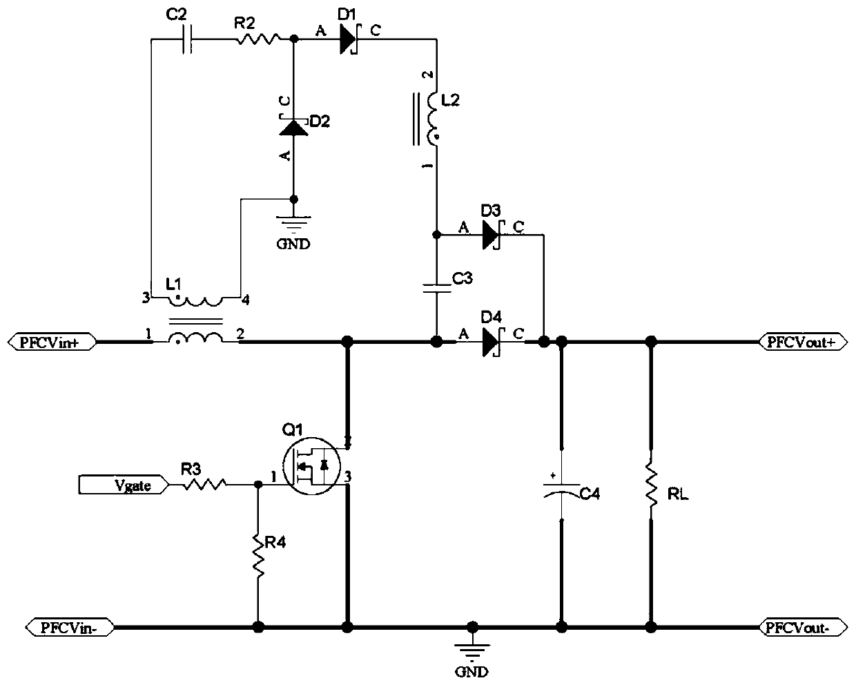
[0012] A lossless snubber circuit for an active PFC circuit, such as figure 1 As shown, including PFCVin+, PFCVin-, PFCVin+, PFCVout+, PFCVout-, Vgate, switch Q1, capacitor C2, capacitor C3, capacitor C4, diode D1, diode D2, diode D3, diode D4, resistor R2, inductor L2 and winding L1, the drain of the switching tube Q1 is respectively connected to one end of the capacitor C3, the anode of the diode D4 and the winding L1, the diode D4 is connected in parallel with the diode D3, and the other end of the capacitor C3 is respectively connected to the winding L1. The diode D3 is connected to on...


PUM


Abstract

The present invention relates to the technical field of circuit structures, in particular to a non-destructive absorption circuit of an active PFC circuit. The non-destructive absorption circuit includes a switching transistor Q1, a capacitor C2, a capacitor C3, a capacitor C4, a diode D1, a diode D2, a diode D3, a diode D4, a resistor R2, an inductor L2, and a winding L1. A drain of the switchingtransistor Q1 is respectively connected to one end of the capacitor C3, an anode of the diode D4, and the winding L1. The diode D4 is connected to the diode D3 in parallel. The capacitor C3 is connected to the diode D3 and the inductor L2. The inductor L2 is connected to the diode D1. The diode D1 is respectively connected to the diode D2 and resistor R2. In the present invention, an interferencesource generated when the power switching transistor works can be better reduced, so that an EMI circuit is simplified, a voltage stress of the power switching transistor is reduced, output efficiency of the whole machine is improved. The circuit is simple to implement with an excellent effect and high reliability.

Description

technical field [0001] The invention relates to the technical field of circuit structures, in particular to a non-destructive absorption circuit of an active PFC circuit. Background technique [0002] At present, under the condition that switching power supply has higher and higher requirements on power factor PF, the PFC circuit of switching power supply needs to use active PFC circuit to achieve higher PF value, and the power switch tube of active PFC circuit works at high frequency On -Off state of fast cycle switching, DV / DT and DI / DT are changing rapidly, so for EMI, the PFC power switch is not only the main interference source of electric field coupling, but also the main interference source of magnetic field coupling, plus the PCB on the The parasitic inductance will generate a peak voltage between the D pole and the S pole when the power switch tube is turned off. The larger the parasitic inductance will be, the higher the peak voltage will be. The traditional method...

Claims


Application Information

Patent Timeline
Patent Type & Authority Applications(China)
IPC IPC(8): H02M1/42
CPCH02M1/4225Y02B70/10
Inventor 廖正民
Owner APM TECH DONGGUAN
Why Eureka
Try Eureka