Light emitting device, manufacturing method thereof, mask plate, display substrate and display device

A technology of light-emitting devices and manufacturing methods, which can be applied to semiconductor devices, electric solid-state devices, electrical components, etc., and can solve problems such as the influence of light-emitting layers

Active Publication Date: 2019-08-20
BOE TECH GRP CO LTD +1
View PDF4 Cites 1 Cited by
  • Summary
  • Abstract
  • Description
  • Claims
  • Application Information

AI Technical Summary

Problems solved by technology

[0005] The present application provides a display device and its manufacturing method, mask plate, display substrate and device, which can solve the problem that impurity particles will affect the light emission of the light-emitting layer. The technical solution is as follows:

Method used


Image

  • Light emitting device, manufacturing method thereof, mask plate, display substrate and display device
  • Light emitting device, manufacturing method thereof, mask plate, display substrate and display device
  • Light emitting device, manufacturing method thereof, mask plate, display substrate and display device

Examples


Embodiment Construction

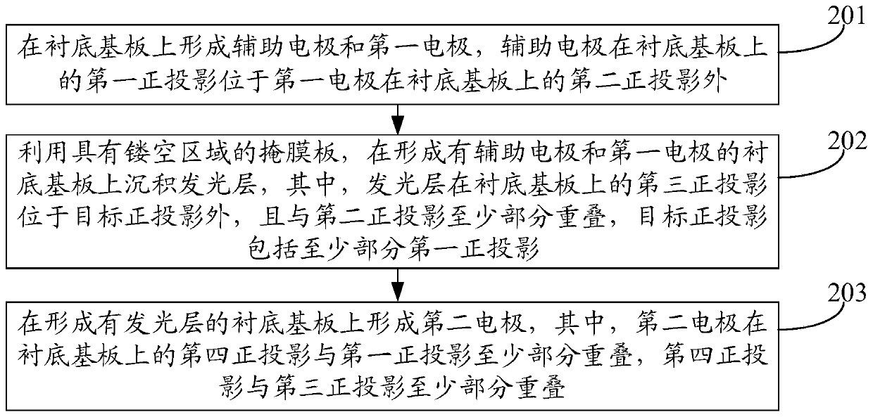
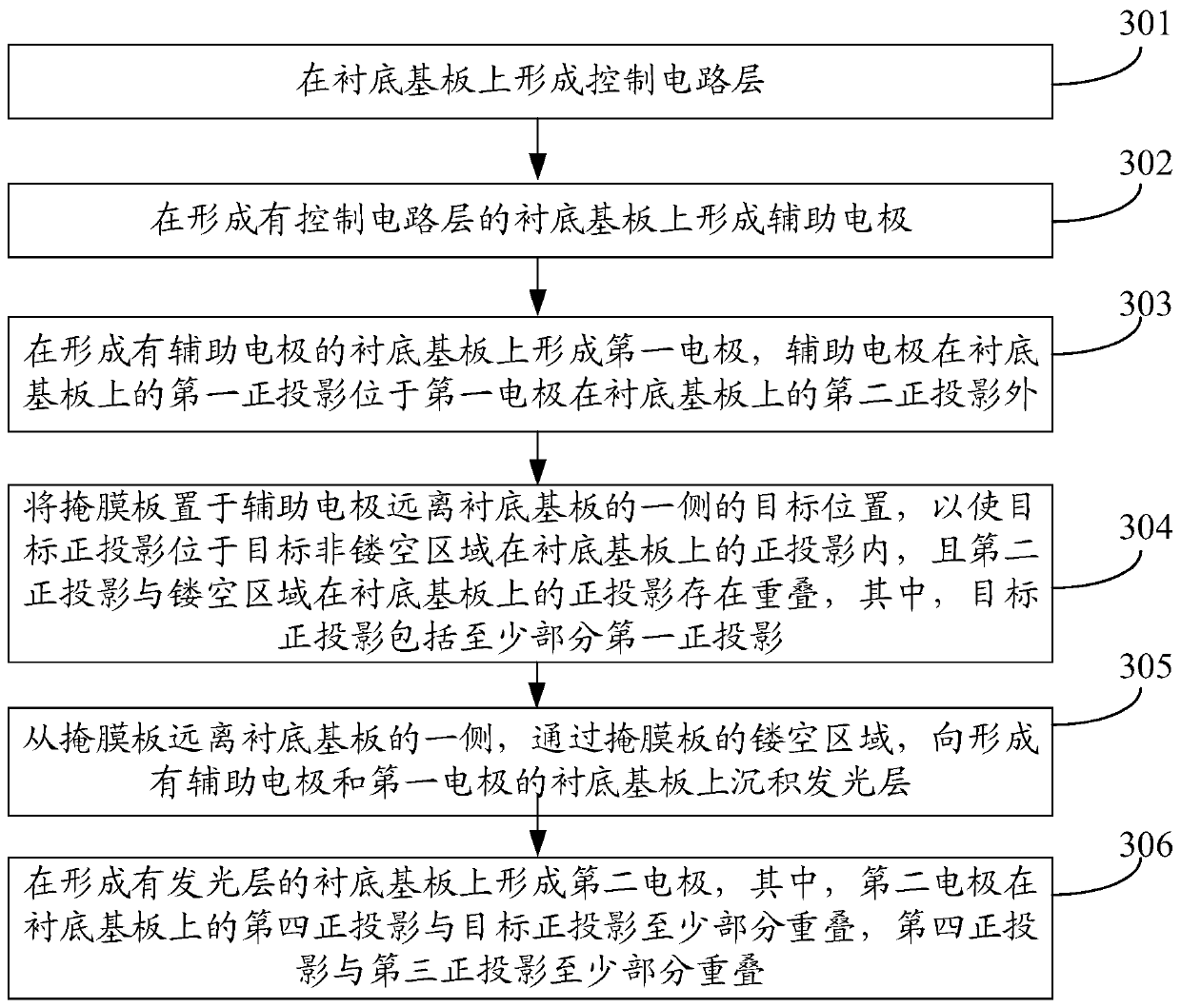
[0043] In order to make the purpose, technical solution and advantages of the present application clearer, the implementation manners of the present application will be further described in detail below in conjunction with the accompanying drawings.

[0044] figure 1 A schematic structural diagram of an OLED display device in the related art is shown. Such as figure 1 As shown, the OLED display device 01 includes: a display substrate ( figure 1 Not marked in ), cover plate 012, black matrix 013, color filter 014, upper cover layer 015, support pillar 016, filling layer 017 and sealant ( figure 1 not shown).

[0045] Wherein, the display substrate includes a light-emitting device 011, and the light-emitting device 011 includes: a base substrate 0111, a control circuit layer 0112, an OLED and an auxiliary electrode 0113, and the OLED includes an anode 0114 and a light-emitting layer 0115 arranged in sequence along a direction away from the base substrate 0111. and cathode 01...


PUM


Abstract

The invention discloses a light emitting device, a manufacturing method thereof, a mask plate, a display substrate and a display device, and belongs to the technical field of display. The method comprises the steps of forming an auxiliary electrode and a first electrode on a substrate, wherein the first orthographic projection of the auxiliary electrode on the substrate is located outside the second orthographic projection of the first electrode on the substrate; depositing a light emitting layer on the substrate with the auxiliary electrode and the first electrode by using the mask plate witha hollowed-out area; and forming a second electrode on the substrate with the light emitting layer. The method solves a problem that impurity particles will affect the light emission of the light emitting layer, and enables the light emitting effect of the light emitting device not to be affected by the impurity particles. The method is applied to the display device.

Description

technical field [0001] The present application relates to the field of display technology, in particular to a display device, a manufacturing method thereof, a mask plate, a display substrate and a device. Background technique [0002] An organic light-emitting diode (English: Organic Light-Emitting Diode; abbreviation: OLED) display device has been widely used due to its better display effect. [0003] In the related art, an OLED display device includes: a light-emitting device, the light-emitting device includes: a base substrate, an insulating layer, an OLED, and an auxiliary electrode, and the OLED includes an anode, a light-emitting layer, and a cathode arranged in sequence along a direction away from the base substrate. Both the auxiliary electrode and the insulating layer are located between the base substrate and the light-emitting layer of the OLED, and are sequentially arranged along a direction away from the base substrate. Moreover, the cathode of the OLED is el...

Claims


Application Information

Patent Timeline
IPC IPC(8): H01L27/32
CPCH10K59/123H10K59/1213H10K59/1201H10K59/80522H10K50/11H10K71/166H10K50/824H10K71/621
Inventor 苏同上王东方刘军胡迎宾王庆贺杜生平闫梁臣
Owner BOE TECH GRP CO LTD
Why Eureka
Try Eureka