
LCD display panel, manufacturing method thereof, and terminal equipment

A technology for display panels and color filter substrates, which is used in printing image acquisition, instruments, computing, etc., can solve the problems of many lines, small effective use of LCD display panels, and inability to apply LCD display panels, etc., to achieve full-screen fingerprint recognition. Effect

Active Publication Date: 2022-04-15
BOE TECH GRP CO LTD +1
View PDF5 Cites 0 Cited by
  • Summary
  • Abstract
  • Description
  • Claims
  • Application Information

AI Technical Summary

Problems solved by technology

Existing in-screen fingerprint recognition sensors are only suitable for OLED display panels. Ultrasonic fingerprint recognition sensors and infrared fingerprint recognition sensors used in OLED display panels require the design of additional drive circuits. Applying them to LCD display panels will lead to excessive wiring , the LCD display panel has problems such as small effective use of space, so it cannot be applied to the LCD display panel

Method used


Image

  • LCD display panel, manufacturing method thereof, and terminal equipment
  • LCD display panel, manufacturing method thereof, and terminal equipment
  • LCD display panel, manufacturing method thereof, and terminal equipment

Examples


Embodiment Construction

[0058] In order to illustrate the present invention more clearly, the present invention will be further described below in conjunction with preferred embodiments and accompanying drawings. Similar parts in the figures are denoted by the same reference numerals. Those skilled in the art should understand that the content specifically described below is illustrative rather than restrictive, and should not limit the protection scope of the present invention.

[0059] One embodiment of the present invention provides a method for preparing an LCD display panel, comprising:

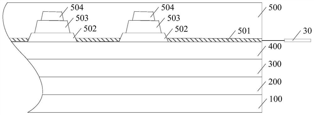
[0060] Step S1, such as figure 1 As shown, a capacitive touch layer 200 is formed on a TFT (Thin Film Transistor, thin film transistor) array substrate 100 .

[0061] Wherein, the method for forming the touch layer 200 can adopt the OGS process known in the art to separately form the capacitive touch layer 200 and bond it with the TFT array substrate 100 .

[0062] in addition, figure 1 What is represente...


PUM

PropertyMeasurementUnit
thicknessaaaaaaaaaa
thicknessaaaaaaaaaa
thicknessaaaaaaaaaa

Abstract

The invention discloses an LCD display panel, a preparation method thereof, and a terminal device. A specific embodiment of the LCD display panel includes a lower polarizer, a TFT substrate TFT array substrate located on the lower polarizer, a capacitive touch layer located on the TFT substrate, and a liquid crystal layer located on the touch layer and a CF substrate color filter substrate located on the liquid crystal layer, and a touch integrated circuit for controlling the touch layer to perform touch recognition, and the LCD display panel also includes a color filter substrate located on the CF substrate A capacitive fingerprint identification layer; a fingerprint identification integrated circuit, used to control the capacitive fingerprint identification layer for fingerprint identification; and an upper polarizer on the capacitive fingerprint identification layer. This embodiment can realize in-screen fingerprint identification of the LCD display panel.

Description

technical field [0001] The invention relates to the field of display technology. More specifically, it relates to an LCD display panel, a manufacturing method thereof, and a terminal device. Background technique [0002] Currently, LCD display panels do not have an in-screen fingerprint recognition function. Existing in-screen fingerprint recognition sensors are only suitable for OLED display panels. Ultrasonic fingerprint recognition sensors and infrared fingerprint recognition sensors used in OLED display panels require the design of additional drive circuits. Applying them to LCD display panels will lead to excessive wiring , The LCD display panel has problems such as small effective use of space, so it cannot be applied to the LCD display panel. [0003] Therefore, it is necessary to provide a new LCD display panel, its preparation method, and terminal equipment. Contents of the invention [0004] The purpose of the present invention is to provide an LCD display pan...

Claims


Application Information

Patent Timeline
Patent Type & Authority Patents(China)
IPC IPC(8): G02F1/1333G06V40/12
CPCG02F1/13338G06V40/1306
Inventor 禹映雪刘雨杰赵婷婷金美灵
Owner BOE TECH GRP CO LTD
Learn More