Display panel manufacturing method and display panel

A technology for a display panel and a manufacturing method, applied in optics, instruments, nonlinear optics, etc., can solve the problems of reducing the polyimide external expansion area, difficult to increase the screen ratio of the display panel, and the width of the display panel frame, etc. The effect of reducing the external expansion area, increasing the occupied area and improving the flatness

Inactive Publication Date: 2019-08-06
TCL CHINA STAR OPTOELECTRONICS TECH CO LTD
View PDF4 Cites 1 Cited by
  • Summary
  • Abstract
  • Description
  • Claims
  • Application Information

AI Technical Summary

Problems solved by technology

[0006] The invention provides a method for manufacturing a display panel and a display panel, which can improve the smoothness of the polyimide edge, reduce the patterned polyimide expansion area, correspondingly reduce the external expansion area of ​​the frame glue, and optimize the existing frame Designed to solve the technical problem that the frame width of the display panel in the prior art is relatively large, making it difficult to increase the screen-to-body ratio of the display panel

Method used


Image

  • Display panel manufacturing method and display panel
  • Display panel manufacturing method and display panel

Examples


Embodiment Construction

[0026] The following descriptions of the various embodiments refer to the accompanying drawings to illustrate specific embodiments in which the invention may be practiced. The directional terms mentioned in the present invention, such as [top], [bottom], [front], [back], [left], [right], [inside], [outside], [side], etc., are only for reference The orientation of the attached schema. Therefore, the directional terms used are used to illustrate and understand the present invention, but not to limit the present invention. In the figures, structurally similar elements are denoted by the same reference numerals.

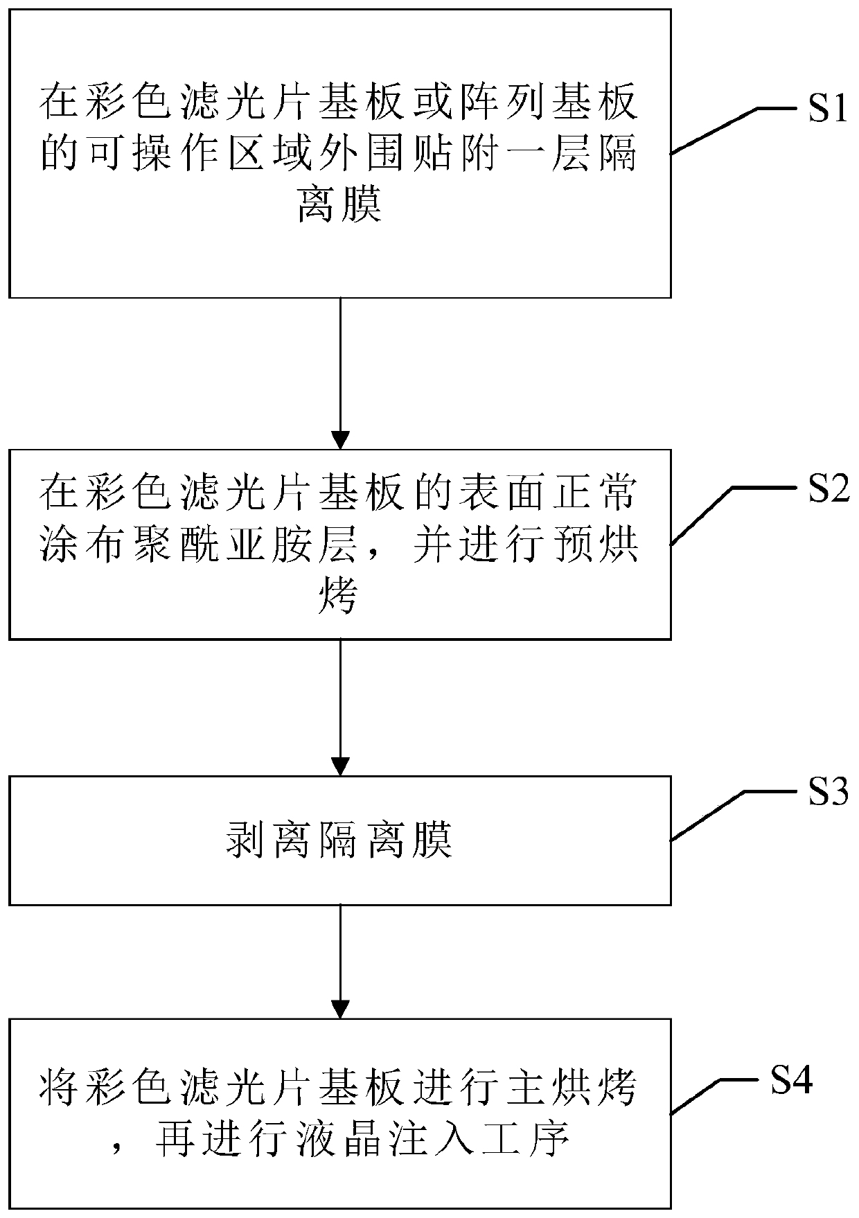
[0027] figure 1 It is a flow chart of a method for manufacturing a display panel according to an embodiment of the present invention, such as figure 1 As shown, the manufacturing method of the display panel includes:

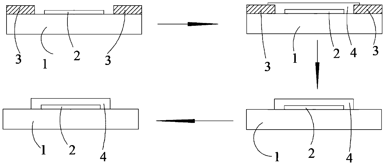
[0028] Step S1: Attach a layer of isolation film 3 on the periphery of the operable area 2 of one of the color filter substrate 1 and the array substr...


PUM

PropertyMeasurementUnit
thicknessaaaaaaaaaa

Abstract

The invention provides a display panel manufacturing method, which comprises the steps of: step S1, attaching a layer of isolating film to the periphery of an operable region of one of a color opticalfilter substrate and an array substrate; step S2, coating a polyimide layer on the surface of the color optical filter substrate and prebaking the surface; S3, peeling off the isolating film; step S4, and performing main baking on the color optical filter substrate, and then performing a liquid crystal injection process. The display panel manufacturing method improves the edge flatness of the polyimide film, shrinks a patterned extension area of the polyimide film, further shrinks an extension region of a frame glue, optimizes the existing frame design, and increases the display scale.

Description

technical field [0001] The present invention relates to the field of display technology, in particular to a method for manufacturing a display panel and the display panel. Background technique [0002] In the manufacturing process of TFT-LCD, an alignment film needs to be provided on the array substrate and the color filter substrate of the TFT-LCD, and the alignment film is processed to form grooves along a certain direction so that the liquid crystals are arranged along the direction of the grooves. Alignment film materials have good chemical corrosion resistance, electrical insulation and other properties. [0003] One of the development trends of thin film transistor liquid crystal display is narrow frame display, which reduces non-display area to increase display ratio. In the existing alignment film (polyimide material) coating process, there are uneven edges of polyimide. The actual polyimide patterning needs to be expanded by 1000~4000um (different polyimide materi...

Claims


Application Information

Patent Timeline
Patent Type & Authority Applications(China)
IPC IPC(8): G02F1/1337G02F1/1333
CPCG02F1/1333G02F1/133723
Inventor 陈皓
Owner TCL CHINA STAR OPTOELECTRONICS TECH CO LTD
Why Eureka
Try Eureka