Automatic appearance inspection system for PCBA (Printed Circuit Board Assembly)

A visual inspection and automatic technology, applied in measuring devices, material analysis by optical means, instruments, etc., can solve the problems of increasing enterprise costs, multi-labor, low PCBA efficiency, etc., so as to increase enterprise costs and improve enterprise income. Effect

Inactive Publication Date: 2019-07-26
武汉辉天同康科技有限公司
View PDF4 Cites 0 Cited by
  • Summary
  • Abstract
  • Description
  • Claims
  • Application Information

AI Technical Summary

Problems solved by technology

[0005] Aiming at the deficiencies of the prior art, the present invention provides a PCBA automatic appearance inspection system, which solves the problem that the existing PCBA appearance inspection method is inefficient and requires more labor, which undoubtedly increases the cost of the enterprise. question

Method used


Image

  • Automatic appearance inspection system for PCBA (Printed Circuit Board Assembly)
  • Automatic appearance inspection system for PCBA (Printed Circuit Board Assembly)
  • Automatic appearance inspection system for PCBA (Printed Circuit Board Assembly)

Examples


Embodiment Construction

[0026] The following will clearly and completely describe the technical solutions in the embodiments of the present invention with reference to the accompanying drawings in the embodiments of the present invention. Obviously, the described embodiments are only some, not all, embodiments of the present invention. Based on the embodiments of the present invention, all other embodiments obtained by persons of ordinary skill in the art without making creative efforts belong to the protection scope of the present invention.

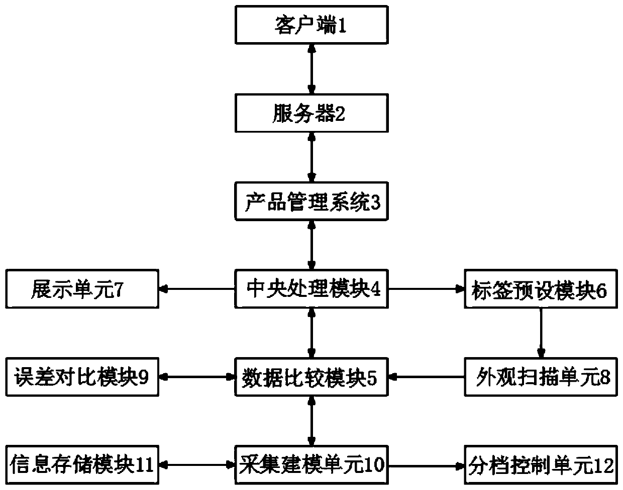
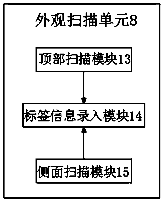
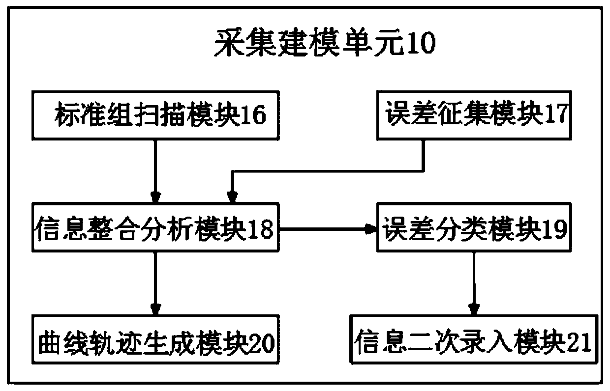
[0027] see Figure 1-5, the embodiment of the present invention provides a technical solution: a PCBA automatic appearance inspection system, including a client 1, a server 2, a product management system 3 and a central processing module 4, the central processing module 4 is an ARM9 series processor, and the client 1 Realize two-way connection with server 2 through Ethernet, server 2 realizes two-way connection with product management system 3 through Ethernet...


PUM


Abstract

The invention discloses an automatic appearance inspection system for a PCBA (Printed Circuit Board Assembly). The system comprises a client side, a server, a product management system and a central processing module, wherein the client side and the server are in bidirectional connection through the Ethernet; the server and the product management system are in bidirectional connection through theEthernet; the product management system and the central processing module are in bidirectional connection through the Ethernet; the central processing module and a data comparison module are in bidirectional connection; and the output end of the central processing module is independently connected with the input end of a tag preset module and the input end of a display unit. The invention relatesto the technical field of PCBA detection. By use of the automatic appearance inspection system for the PCBA, infrared is used for measuring a distance, a standard mode is established, automated equipment is cooperated to carry out information conversion and comparison so as to be simple, clear, practical and efficient, and enterprise income is improved. By use of the system, the problems that enterprise cost is surely increased since an existing PCBA appearance detection way is low in efficiency and simultaneously needs more manpower can be solved.

Description

technical field [0001] The invention relates to the technical field of PCBA detection, in particular to a PCBA automatic appearance inspection system. Background technique [0002] PCBA means that the empty PCB board passes through the SMT upper part, and then goes through the whole process of DIP plug-in. The PCB board is a printed circuit board, also known as a printed circuit board, and a printed circuit board. The provider of the connection. Because it is made using electronic printing techniques, it is called a "printed" circuit board. Before the appearance of printed circuit boards, the interconnection between electronic components relied on the direct connection of wires to form a complete circuit. Now, circuit breadboards only exist as effective experimental tools, and printed circuit boards have already been used in the electronics industry. became an absolute dominator. [0003] The accuracy of the circuit board is very important. In PCBA, due to installation an...

Claims


Application Information

Patent Timeline
Patent Type & Authority Applications(China)
IPC IPC(8): G01N21/956
CPCG01N21/956G01N2021/95638
Inventor 唐凯
Owner 武汉辉天同康科技有限公司
Why Eureka
Try Eureka