
Turnover structure and wafer spin-drying equipment

A technology of flipping structures and wafers, which is applied in the direction of electrical components, semiconductor/solid-state device manufacturing, circuits, etc., can solve problems such as waste of manpower, wafer pollution, and low efficiency of wafer drying equipment, so as to alleviate the problems of low efficiency Effect

Active Publication Date: 2019-07-19
BEIJING SEMICON EQUIP INST THE 45TH RES INST OF CETC
View PDF12 Cites 4 Cited by
  • Summary
  • Abstract
  • Description
  • Claims
  • Application Information

AI Technical Summary

Problems solved by technology

[0005] The purpose of the present invention is to provide a flipping structure to alleviate the technical problems of low efficiency of wafer drying equipment in the prior art, waste of manpower and easy contamination of wafers

Method used


Image

  • Turnover structure and wafer spin-drying equipment
  • Turnover structure and wafer spin-drying equipment
  • Turnover structure and wafer spin-drying equipment

Examples


Embodiment 1

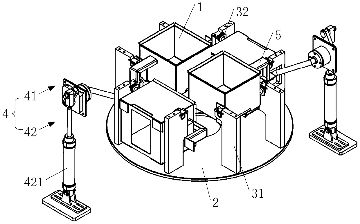
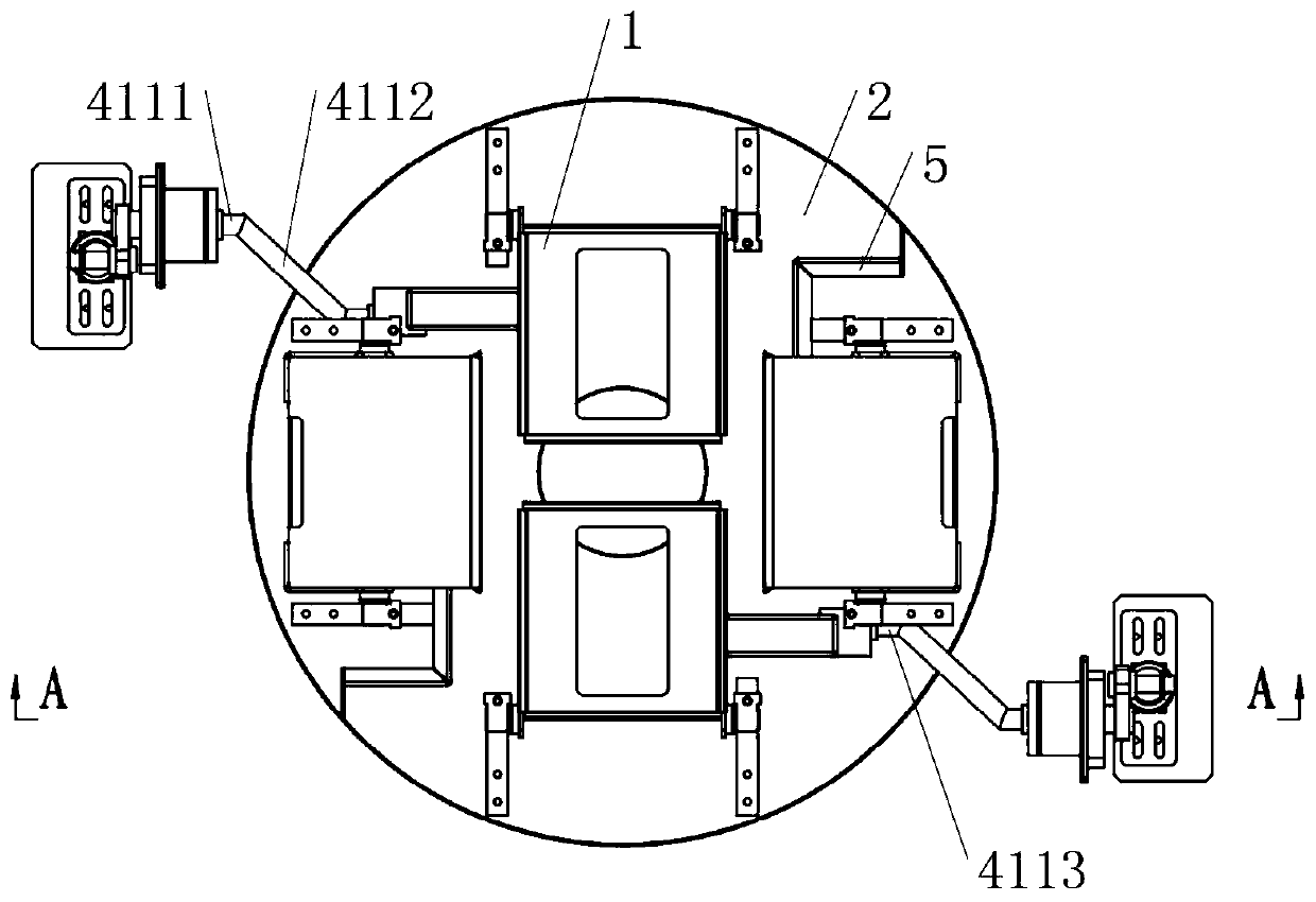
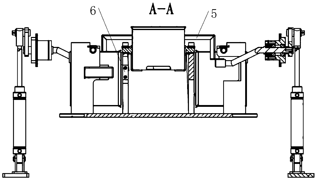
[0051] see Figure 1-Figure 6 As shown, this embodiment provides an inversion structure, which is applied to wafer drying equipment. The inversion structure includes a carrier box 1, a turntable 2 and an inversion device 4; the carrier box 1 is rotatably connected to the turntable 2; the inversion device 4 is driven and connected The carrier box 1 is capable of driving the carrier box 1 to turn over on the turntable 2 .

[0052] It should be noted that when the wafer needs to be dried, the wafer is placed in the carrier box 1. Specifically, the carrier box 1 is driven to rotate relative to the turntable 2 by the turning device 4, so that the carrier box can be turned over. Make the carrier box 1 turn over to facilitate placing the wafer in the carrier box 1; after the wafer is dried, the wafer in the carrier box 1 needs to be taken out, specifically, the carrier box 1 is driven by the turning device 4 Rotating relative to the turntable 2 realizes the overturning of the carrier ...

Embodiment 2

[0076] Embodiment 2 provides a wafer drying equipment. The wafer drying equipment includes the flipping structure of Embodiment 1. The technical features of the flipping structure disclosed in Embodiment 1 are also applicable to this embodiment. The disclosure of Embodiment 1 The technical features of the flip structure will not be described repeatedly. The implementation of the wafer spin-drying equipment will be further described in detail below in conjunction with the accompanying drawings.

[0077] In order to save space, the improved features of this embodiment are also reflected in Figure 1-Figure 6 in, therefore, combined with Figure 1-Figure 6 The configuration of this example will be described.

[0078] see Figure 1-Figure 6 As shown, the wafer drying equipment provided in this embodiment, including the flip structure, further alleviates the technical problems existing in the prior art that the wafer drying equipment has low efficiency, wastes manpower, and easi...


PUM


Abstract

The invention relates to the technical field of semiconductor wafer processing devices, in particular to a turnover structure and wafer spin-drying equipment. The turnover structure is applied to thewafer spin-drying equipment, and comprises a bearing box, a rotary disc and a turnover device; the bearing box is rotationally connected to the rotary disc; and the turnover device is in driving connection with the bearing box and can drive the bearing box to turn over on the rotary disc. The wafer spin-drying equipment comprises the turnover structure. According to the turnover structure and thewafer spin-drying equipment, the technical problems that in the prior art, the wafer spin-drying equipment is relatively low in efficiency, wastes labor and easily causes pollution to wafers are relieved.

Description

technical field [0001] The invention relates to the technical field of semiconductor wafer processing devices, in particular to an inversion structure and wafer drying equipment. Background technique [0002] Wafer refers to the silicon wafer used in the production of silicon semiconductor integrated circuits. Because of its circular shape, it is called a wafer. It can be processed into various circuit element structures on silicon wafers, and become electronic component products with specific electrical functions. With the development of the size of integrated circuits on semiconductor wafers to the micron level, the cleaning requirements in the semiconductor wafer manufacturing process are getting higher and higher, especially if the semiconductor wafers are polluted by dust particles and metals during the manufacturing process, It is easy to cause damage to the function of the circuit in the chip, form a short circuit or an open circuit, etc., resulting in the failure of...

Claims


Application Information

Patent Timeline
IPC IPC(8): H01L21/67
CPCH01L21/67034
Inventor 陈苏伟吴光庆王勇威刘建民安稳鹏
Owner BEIJING SEMICON EQUIP INST THE 45TH RES INST OF CETC
Learn More