Method of embedding opto-electronic components in layer

A technology of optoelectronic devices and embedded layers, which is applied in the direction of electric solid devices, household components, electrical components, etc., can solve the problems of device damage, device overmolding, etc., and achieve the effect of reducing the risk of damage to the device and reducing the extrusion force

Active Publication Date: 2019-07-12
OSRAM OPTO SEMICONDUCTORS GMBH
View PDF7 Cites 0 Cited by
  • Summary
  • Abstract
  • Description
  • Claims
  • Application Information

AI Technical Summary

Problems solved by technology

In this case, however, damage to the component or overmolding of the upper side of the component may result

Method used


Image

  • Method of embedding opto-electronic components in layer
  • Method of embedding opto-electronic components in layer
  • Method of embedding opto-electronic components in layer

Examples


Embodiment Construction

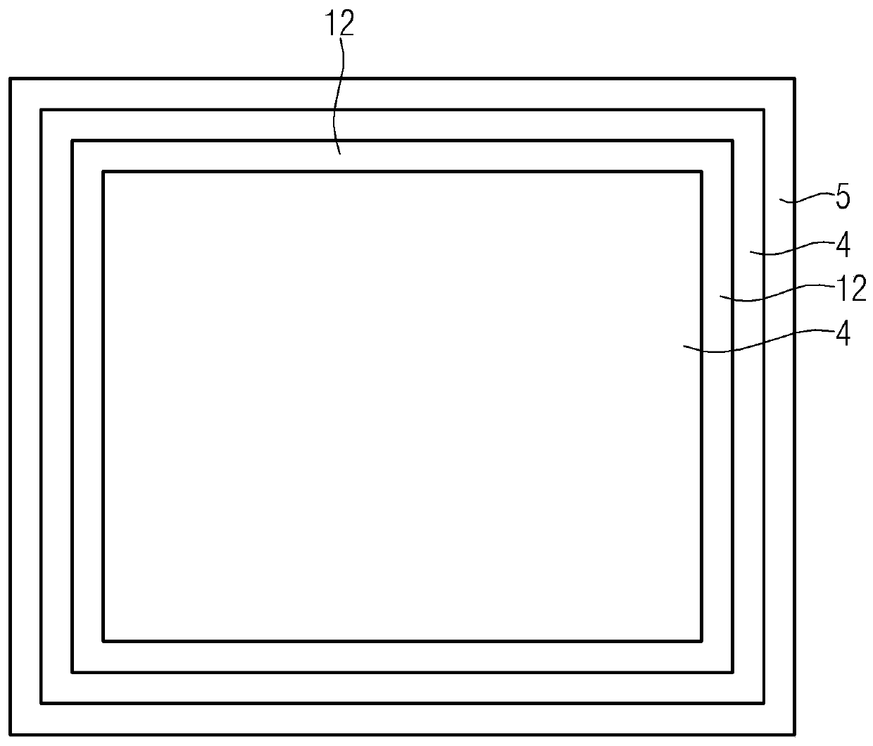
[0034] figure 1 A schematic sectional view through the device for embedding an optoelectronic component 1 in a layer is shown. A forming tool 2 is provided which, in the exemplary embodiment shown, has a cover plate 3 and a carrier plate 4 . Furthermore, a film 5 is arranged on the underside of the carrier plate 4 . The film 5 here covers the entire underside of the carrier plate 4 and is thus arranged between the carrier plate 4 and the component 1 . Depending on the chosen embodiment, the membrane 5 can be dispensed with. The optoelectronic component 1 is designed, for example, as a radiation component. For example, the optoelectronic component 1 can be designed in the form of a light-emitting diode. The component 1 is arranged on a carrier 6 . In the exemplary embodiment shown, the carrier plate 4 is made of elastic material. For example, the carrier plate 4 can be made of spring steel. The carrier plate 4 has an underside 7 which is substantially flat under no load....


PUM


Abstract

The invention relates to a molding tool and a method of embedding opto-electronic components in a layer, wherein the components are disposed beside one another to be spaced apart on a carrier, and themethod comprises the steps: providing a molding tool having a bearing plate, wherein the bearing plate on a lower side includes resilient bearing regions, bringing the bearing plate by way of the resilient bearing regions to bear on upper sides of the components, filling an intermediate space between the components, the carrier, and the bearing plate with a molding material, curing the molding material to form the layer, and removing the molding tool from the layer and the embedded components.

Description

technical field [0001] The invention relates to a method for embedding optoelectronic components in layers and a forming tool for carrying out the method. Background technique [0002] It is known from the prior art to embed optoelectronic components in layers by means of injection molding methods or film-assisted molding methods. In this case, however, damage to the component or overmolding of the top side of the component can result. Contents of the invention [0003] It is an object of the present invention to provide an improved method for embedding optoelectronic components in layers. Furthermore, it is an object of the invention to provide an improved forming tool for embedding optoelectronic components in layers. [0004] Said object is achieved by the independent claims. [0005] The proposed method has the advantage that the pressing force on the component is reduced and that molding material is nevertheless reliably prevented from being applied to the top of t...

Claims


Application Information

Patent Timeline
IPC IPC(8): H01L21/56H01L25/075H01L33/52B29C39/10
CPCH01L21/565H01L25/0753H01L33/52B29C39/10B29L2031/747B29C33/42B29L2031/34B29C45/14639B29C45/26B29C2045/14098B29C2033/0094B29C2045/14163B29C33/14B29C45/14836B29D11/00807B29L2031/3481
Inventor 彼得·纳格尔托比亚斯·格布赫尔
Owner OSRAM OPTO SEMICONDUCTORS GMBH
Why Eureka
Try Eureka