
A Method for Minimum Switching Loss of Three-phase Inverter Based on Dual Carrier and Synthetic Modulation Wave

A three-phase inverter, switching loss technology, applied in the direction of output power conversion device, AC power input conversion to DC power output, electrical components, etc., to achieve the effect of optimizing switching loss

Active Publication Date: 2020-07-03
上海宝准电源科技有限公司 +2
View PDF6 Cites 0 Cited by
  • Summary
  • Abstract
  • Description
  • Claims
  • Application Information

AI Technical Summary

Problems solved by technology

However, the traditional DPWM can only achieve the minimum switching loss within a specific power factor range. When the power factor range is further reduced, the above method cannot reduce the switching loss to a certain extent, but it is not the optimal method, and the switching loss still exists. room for optimization

Method used


Image

  • A Method for Minimum Switching Loss of Three-phase Inverter Based on Dual Carrier and Synthetic Modulation Wave
  • A Method for Minimum Switching Loss of Three-phase Inverter Based on Dual Carrier and Synthetic Modulation Wave
  • A Method for Minimum Switching Loss of Three-phase Inverter Based on Dual Carrier and Synthetic Modulation Wave

Examples


Embodiment Construction

[0040] The present invention discloses a method for minimum switching loss of a three-phase inverter based on dual-carrier and synthesized modulation waves. The specific implementation of the present invention will be further described below in combination with preferred embodiments.

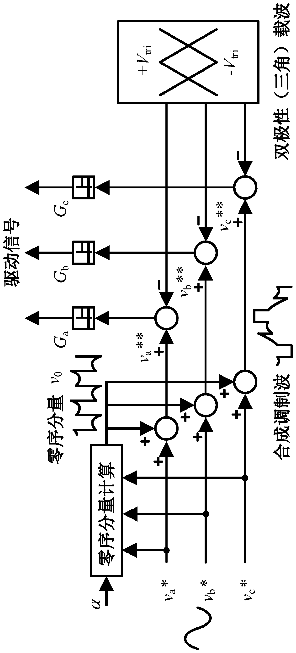
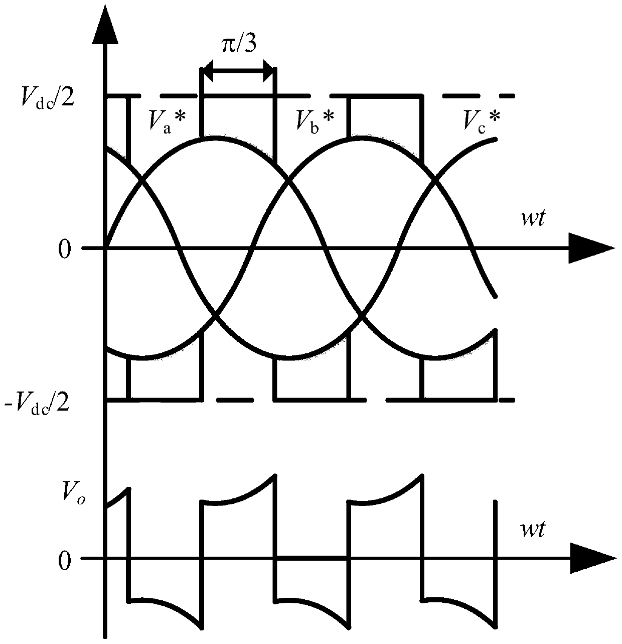
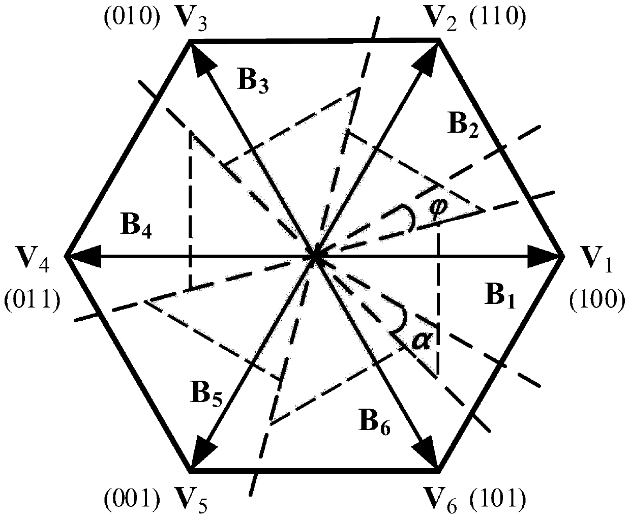
[0041] see attached Figure 1 to Figure 5 , figure 1 The waveform modulation process of the zero-sequence component, sine wave and bipolar carrier wave of the three-phase inverter minimum switching loss method based on dual carrier and synthetic modulation wave is shown, figure 2 A schematic diagram showing the synthesis of zero-sequence voltage components and sine waves of the three-phase inverter minimum switching loss method based on dual-carrier and synthetic modulation waves, Figure 3A , Figure 3B with Figure 3C The sector assignments in the voltage space vector diagram are shown, respectively, Figure 4A with Figure 4B The comparison of the loss characteristics between this metho...


PUM


Abstract

The invention discloses a three-phase inverter least switching loss method based on dual-carrier and synthetic modulation wave. The method comprises the following steps: S1, superposing a zero-sequence component on a sine modulation wave to form the synthetic modulation wave in a modulation way; and step S2, superposing the synthetic modulation wave on the bipolar carrier to form a driving signalGa, a driving Gb and a driving signal Gc in the modulation way. Through the three-phase inverter least switching loss method based on the dual-carrier and the synthetic modulation wave, the defect that the traditional DPWM can realize the least switching loss only in the specific power factor range is avoided by adopting the bipolar carrier and the least switching loss PWM strategy based on the zero sequence component and the sine wave synthetic modulation wave, so that the switching loss can be further optimized when the power factor range is further reduced, thereby realizing the switching loss least discontinuous modulation strategy DPWM in the full power factor range.

Description

technical field [0001] The invention belongs to the technical field of power electronics, and in particular relates to a method for minimum switching loss of a three-phase inverter based on dual carrier waves and synthesized modulation waves. Background technique [0002] With the rapid development of power electronics technology, three-phase voltage source inverters are widely used in the fields of AC motor drives, power quality and new energy power generation. Switching loss is the main factor restricting the improvement of inverter efficiency. In order to improve the efficiency and power density of the inverter, it is necessary to effectively reduce the switching loss of the inverter. In the conventional carrier modulation SPWM method, the triangular carrier and the sinusoidal modulation wave are compared to achieve. Discontinuous modulation DPWM is realized by injecting a specific shape of zero-sequence components into the modulation wave, which can reduce the switching...

Claims


Application Information

Patent Timeline
Patent Type & Authority Patents(China)
IPC IPC(8): H02M7/5387H02M7/5395
Inventor 梁光耀宋加旺刘广财刘红伟
Owner 上海宝准电源科技有限公司
Learn More