


Quick Research
Generate reliable direction feasibility study reports for your R&D in just a few steps.

Technical Q&A
Discover and master advanced knowledge NOW. Basics, ideas, possibilities, all at once.

Find Solutions
As an expert in R&D theories, this can generate solutions to your technical problems instantly.

Evaluate Feasibility
Analyze your overall solution with one click, know your potential R&D risks in advance.

Monitor Landscape
Get weekly tech updates, stay abreast of the latest tech innovations and key insights.
Display substrate, preparation method thereof and display device
A technology of display substrate and display structure, which is used in static indicators, semiconductor/solid-state device manufacturing, optics, etc., and can solve problems such as the inability to achieve borderless display screens.
- Summary
- Abstract
- Description
- Claims
- Application Information
AI Technical Summary
Problems solved by technology
Method used
Image

Examples
Embodiment 1
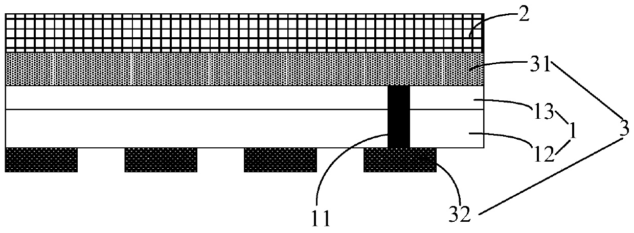
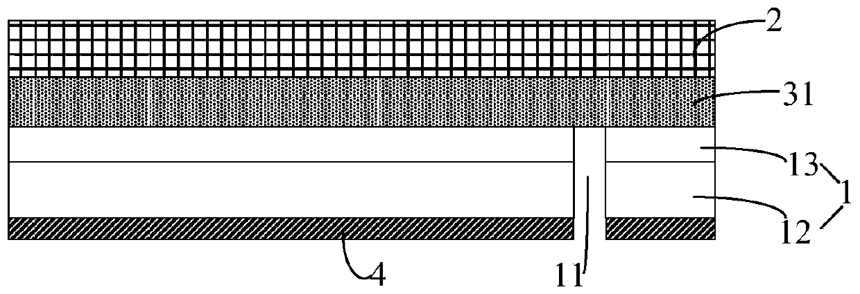
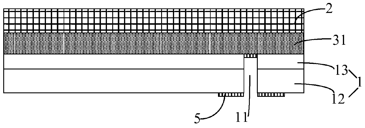
[0033] This embodiment provides a display substrate, such as figure 1 As shown, it includes: a base structure 1 and a display structure 2 arranged above the base structure 1. The display substrate also includes a driving circuit 3 for driving the display structure 2 to display. The driving circuit 3 includes a TFT circuit 31 and a peripheral circuit 32. The TFT circuit 31 is arranged between the base structure 1 and the display structure 2, the peripheral circuit 32 is used to drive the TFT circuit 31, the peripheral circuit 32 is arranged on the side of the base structure 1 away from the display structure 2, and the peripheral circuit 32 is located on the base of the display structure 2 In the orthographic projection area on the structure 1 , the peripheral circuit 32 is connected to the TFT circuit 31 through the via hole 11 opened in the base structure 1 .
[0034] Wherein, the peripheral circuit 32 refers to the part of the driving circuit used to drive the TFT circuit, an...
Embodiment 2
[0057] This embodiment provides a display substrate. The difference from Embodiment 1 is that the display structure includes a plurality of liquid crystal pixel units. That is, the display substrate is a liquid crystal display substrate.
[0058] Wherein, a plurality of liquid crystal pixel units are arranged in an array. The specific structure of the liquid crystal display structure is an existing relatively mature technology, and will not be repeated here.
[0059] Other structures and preparation methods of the display substrate in this embodiment are the same as those in Embodiment 1, and details are not repeated here.
[0060] Beneficial effects of embodiment 1-2: the display substrate provided by embodiment 1-2, by arranging the peripheral circuit originally arranged in the frame area of the display substrate in the driving circuit on the side of the base structure away from the display structure, and making it Located in the area of the orthographic projection of ...
Embodiment 3
[0062] This embodiment provides a display device, including the display substrate in Embodiment 1 or 2.
[0063] By using the display substrate in Embodiment 1 or 2, the display device can realize borderless display, which is beneficial to realize the seamless splicing display of the display device.
[0064] The display device provided by the present invention can be any product or component with display function such as LCD panel, LCD TV, OLED panel, OLED TV, display, mobile phone, navigator, etc., and can also be a semi-finished product of the above-mentioned product or component with display function pieces.
PUM
 Abstract
Description
Claims
Application Information
 - R&D Engineer
- R&D Manager
- IP Professional
- Industry Leading Data Capabilities
- Powerful AI technology
- Patent DNA Extraction
Browse by: Latest US Patents, China's latest patents, Technical Efficacy Thesaurus, Application Domain, Technology Topic, Popular Technical Reports.
© 2024 PatSnap. All rights reserved.Legal|Privacy policy|Modern Slavery Act Transparency Statement|Sitemap|About US| Contact US: help@patsnap.com