Selective absorption enhanced wide-spectrum multi-band detection structure and preparation method thereof

A wide-spectrum, selective technology, applied in the field of photoelectric detection, to achieve the effect of improving detection efficiency and sensitivity, and improving light wave utilization

Active Publication Date: 2019-06-14
XIAN TECHNOLOGICAL UNIV
View PDF7 Cites 9 Cited by
  • Summary
  • Abstract
  • Description
  • Claims
  • Application Information

AI Technical Summary

Problems solved by technology

[0005] The purpose of the present invention is to provide a selective absorption enhanced wide-spectrum multi-band detection structure and its preparation method to solve the problem that the detector structure in the prior art cannot simultaneously realize visible light-near-infrared multi-band absorption enhanced detection

Method used


Image

  • Selective absorption enhanced wide-spectrum multi-band detection structure and preparation method thereof
  • Selective absorption enhanced wide-spectrum multi-band detection structure and preparation method thereof
  • Selective absorption enhanced wide-spectrum multi-band detection structure and preparation method thereof

Examples


Embodiment Construction

[0024] The present invention will be described in detail below in conjunction with the accompanying drawings and specific embodiments.

[0025] The basic principles and ideas of this application are:

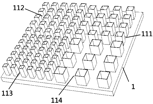
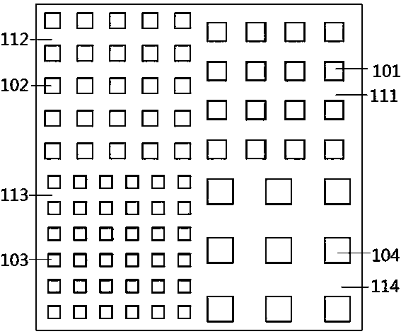
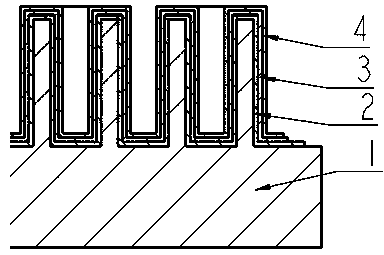
[0026] The base of the wide-spectrum detection structure is an array of three-dimensional square well microstructures, and there are resonant cavities in the square well microstructures and between the square well microstructures. A microlens array is arranged above the subpixel unit composed of the square well microstructure array and the lower electrode 2 on its surface, the photosensitive layer 3 and the upper electrode 4, and each microlens is opposite to the subpixel unit below, and the microlens will incident The light waves converge, pass through the filter, and enter the wide-spectrum detection structure. Most of the light waves hit the resonant cavity, and a small part hit the non-resonant place. The incident light wave passes through the upper electrode 4 which is con...


PUM


Abstract

The invention relates to a selective absorption enhanced wide-spectrum multi-band detection structure and a preparation method thereof. The selective absorption enhanced wide-spectrum multi-band detection structure comprises a plurality of sub-pixel units capable of detecting incident light of different bands, each sub-pixel unit is composed of a square well-shaped microstructure array and a metallower electrode, a photosensitive layer and an upper electrode on the surface of the microstructure array, the size and array spacing of the square well-shaped microstructures in different sub-pixelunits are determined according to the detection bands of the sub-pixel units where the microstructures are located, the square well-shaped microstructure is provided with an opened upper end and a hollow inside to form a resonant cavity, and the adjacent square well-shaped microstructures in the same sub-pixel unit form a resonant cavity. The scheme of the invention solves the problem that a detector structure in the prior art cannot simultaneously realize visible light-near-infrared multi-band absorption enhanced detection.

Description

technical field [0001] The invention belongs to the technical field of photoelectric detection, and in particular relates to a selective absorption enhanced wide-spectrum multi-band detection structure and a preparation method thereof. Background technique [0002] Photodetectors are detected by changes in the conductivity of the irradiated material caused by radiation. Photodetectors have a wide range of uses. They are mainly used in imaging and detection, industrial automatic control, photometry, etc. in the visible or near-infrared band; in the infrared band, they are mainly used in infrared thermal imaging, infrared remote sensing, etc. The common ones are single-band visible light imaging or single-band infrared imaging devices, which have narrow band coverage and low integration. In the application of wide-spectrum detection, they are large in size, heavy in weight, high in power consumption, and not high enough for the utilization of incident light waves. Because of ...

Claims


Application Information

Patent Timeline
IPC IPC(8): H01L27/146
CPCH01L27/14621H01L27/1463H01L27/14601H01L27/1461H01L27/14629
Inventor 刘欢刘卫国安妍白民宇韩军王卓曼胡加兴蔡长龙
Owner XIAN TECHNOLOGICAL UNIV
Why Eureka
Try Eureka