


Quick Research
Generate reliable direction feasibility study reports for your R&D in just a few steps.

Technical Q&A
Discover and master advanced knowledge NOW. Basics, ideas, possibilities, all at once.

Find Solutions
As an expert in R&D theories, this can generate solutions to your technical problems instantly.

Evaluate Feasibility
Analyze your overall solution with one click, know your potential R&D risks in advance.

Monitor Landscape
Get weekly tech updates, stay abreast of the latest tech innovations and key insights.
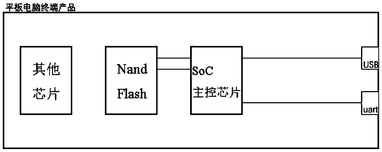
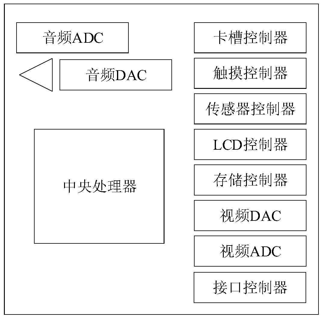
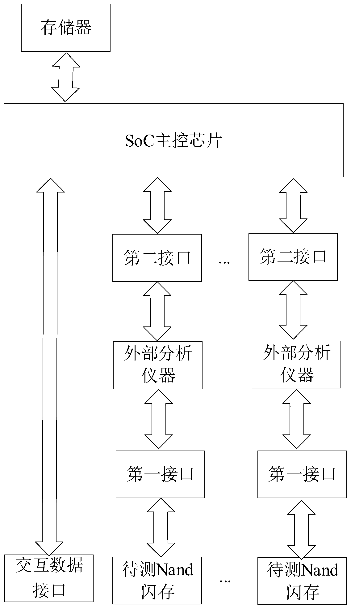
A Nand flash memory analysis device and method based on a SoC main control chip
A technology of a main control chip and an analysis device, applied in the field of flash memory storage, can solve problems such as inability to analyze Nand flash memory quickly and effectively, and achieve the effects of simple design, high versatility and low price
- Summary
- Abstract
- Description
- Claims
- Application Information
AI Technical Summary
Problems solved by technology
Method used
Image

Examples
Embodiment Construction
[0040] In the following, the concept, specific structure and technical effects of the present invention will be clearly and completely described in conjunction with the embodiments and the drawings, so as to fully understand the objectives, solutions and effects of the present invention. It should be noted that the embodiments in the application and the features in the embodiments can be combined with each other if there is no conflict. The same reference numerals used throughout the drawings indicate the same or similar parts.
[0041] It should be noted that, unless otherwise specified, when a feature is called "fixed" or "connected" to another feature, it can be directly fixed and connected to another feature, or indirectly fixed or connected to another feature. One feature. In addition, the top, bottom, left, right and other descriptions used in this application are only relative to the mutual positional relationship of the various components of the application in the drawin...
PUM
 Abstract
Description
Claims
Application Information
 - R&D Engineer
- R&D Manager
- IP Professional
- Industry Leading Data Capabilities
- Powerful AI technology
- Patent DNA Extraction
Browse by: Latest US Patents, China's latest patents, Technical Efficacy Thesaurus, Application Domain, Technology Topic, Popular Technical Reports.
© 2024 PatSnap. All rights reserved.Legal|Privacy policy|Modern Slavery Act Transparency Statement|Sitemap|About US| Contact US: help@patsnap.com