


Quick Research
Generate reliable direction feasibility study reports for your R&D in just a few steps.

Technical Q&A
Discover and master advanced knowledge NOW. Basics, ideas, possibilities, all at once.

Find Solutions
As an expert in R&D theories, this can generate solutions to your technical problems instantly.

Evaluate Feasibility
Analyze your overall solution with one click, know your potential R&D risks in advance.

Monitor Landscape
Get weekly tech updates, stay abreast of the latest tech innovations and key insights.
Flat-panel liquid crystal antenna and manufacturing method thereof
A production method and liquid crystal technology, applied in antennas, nonlinear optics, printed circuit manufacturing, etc., can solve the problems of bulkiness, high cost, and easy damage, and achieve the effects of reducing manufacturing costs, improving manufacturing efficiency, and saving busy waiting
- Summary
- Abstract
- Description
- Claims
- Application Information
AI Technical Summary
Problems solved by technology
Method used
Image

Examples
Embodiment 1
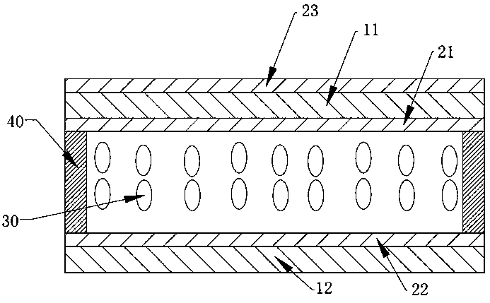
[0041] Such as figure 1 As shown, it is Embodiment 1 of the present invention, and this specific embodiment provides a flat liquid crystal antenna. The flat liquid crystal antenna includes a first substrate 11 and a second substrate 12 oppositely arranged, and also includes a liquid crystal layer 30 between the first substrate 11 and the second substrate 12 .
[0042] The first substrate 11 and the second substrate 12 are selected from materials with good stability and insulation effect and extremely low dielectric loss. In this embodiment, the first substrate 11 and the second substrate 12 are rigid substrates, which can be glass substrates. materials, fused silica, ceramic substrates, and ceramic thermoset polymer composites.
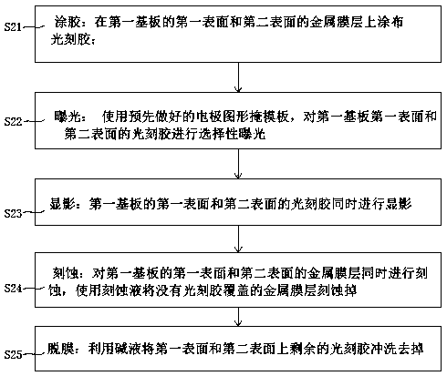
[0043] A first metal film layer 21 is disposed on the first surface of the first substrate 11 facing the second substrate 12 . The first metal film layer 21 is a patterned first metal film layer. The patterned first metal film layer 21 includes a f...
Embodiment 2
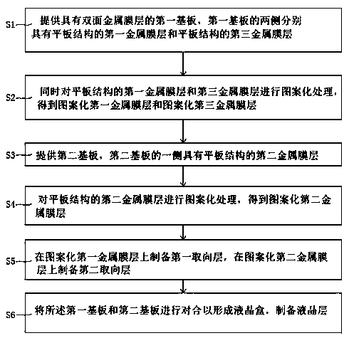
[0083] This specific embodiment provides a method for manufacturing a flat liquid crystal antenna, which is used to make the flat liquid crystal antenna described in Embodiment 1. The manufacturing method includes the following steps:
[0084] S1: providing a first substrate 11 with a double-sided metal film layer, the two sides of the first substrate 11 respectively have a first metal film layer 21 with a planar structure and a third metal film layer 23 with a planar structure;
[0085] S2: Simultaneously patterning the double-sided metal: patterning the first metal film layer 21 and the third metal film layer 23 of the planar structure at the same time to obtain the patterned first metal film layer 21 and the patterned third metal film layer. Metal film layer 23;
[0086] S3: providing a second substrate 12, one side of the second substrate 12 has a second metal film layer 22 with a planar structure;
[0087] S4: Patterning the second metal film layer 22 with a planar struc...
PUM
| Property | Measurement | Unit |
|---|---|---|
| thickness | aaaaa | aaaaa |
Abstract
Description
Claims
Application Information
 - R&D Engineer
- R&D Manager
- IP Professional
- Industry Leading Data Capabilities
- Powerful AI technology
- Patent DNA Extraction
Browse by: Latest US Patents, China's latest patents, Technical Efficacy Thesaurus, Application Domain, Technology Topic, Popular Technical Reports.
© 2024 PatSnap. All rights reserved.Legal|Privacy policy|Modern Slavery Act Transparency Statement|Sitemap|About US| Contact US: help@patsnap.com