Circuit board and manufacturing method thereof

A manufacturing method and circuit board technology, which is applied in the direction of printed circuit manufacturing, printed circuit, printed circuit components, etc., can solve the problems of many times of pressing and long production cycle of products, and achieve the goal of reducing the number of times of pressing and shortening the production cycle Effect

Active Publication Date: 2020-07-17
TRIPOD WUXI ELECTRONICS
View PDF6 Cites 0 Cited by
  • Summary
  • Abstract
  • Description
  • Claims
  • Application Information

AI Technical Summary

Problems solved by technology

Furthermore, since the multilayer stacking method of laser holes needs to be increased layer by layer, the number of laminations required for the manufacturing process is large and the production cycle of the product is long

Method used


Image

  • Circuit board and manufacturing method thereof
  • Circuit board and manufacturing method thereof
  • Circuit board and manufacturing method thereof

Examples


Embodiment Construction

[0056] see Figure 1 to Figure 14 , is an embodiment of the present invention. It should be explained first that this embodiment corresponds to the relevant quantities and shapes mentioned in the drawings, and is only used to specifically illustrate the implementation of the present invention, so as to facilitate the understanding of the content of the present invention. It is not intended to limit the protection scope of the present invention.

[0057] [Manufacturing method of circuit board]

[0058] Such as Figure 1 to Figure 12 , this embodiment discloses a method for manufacturing a circuit board. The manufacturing method of the circuit board includes steps S101 to S108. It must be noted that the order of the steps and the actual operation mode described in this embodiment can be adjusted according to requirements, and are not limited to the description in this embodiment.

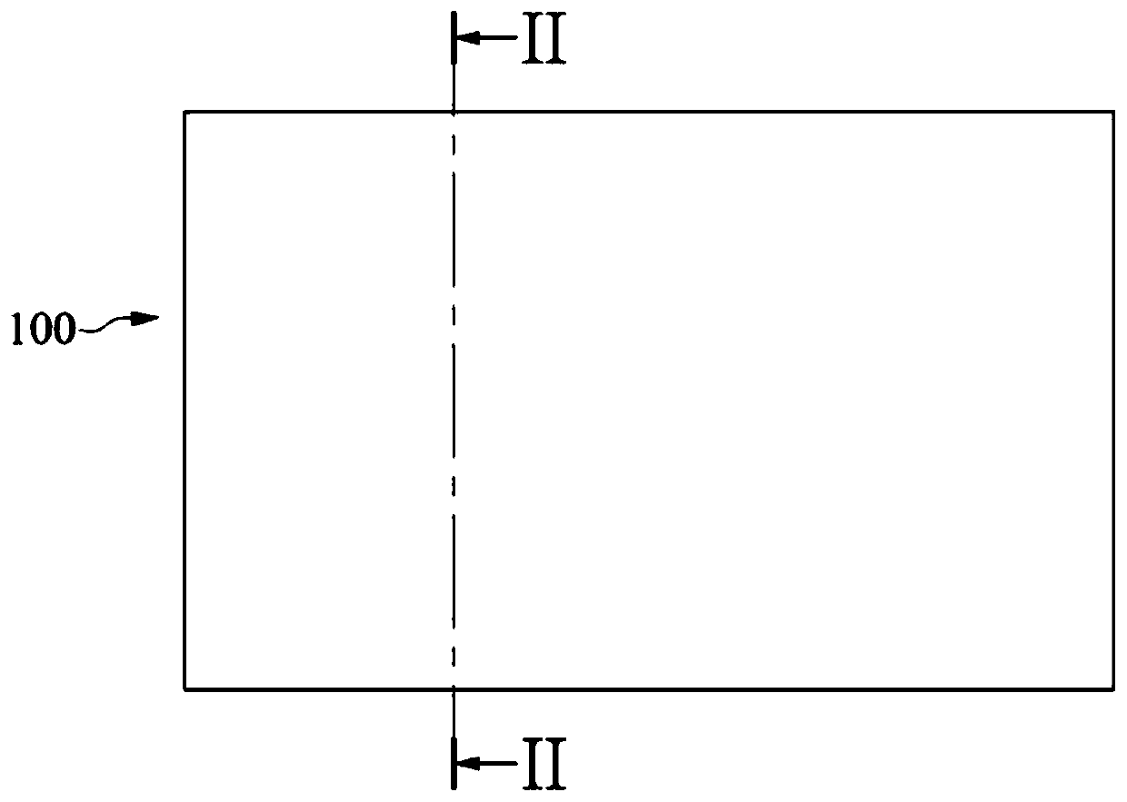
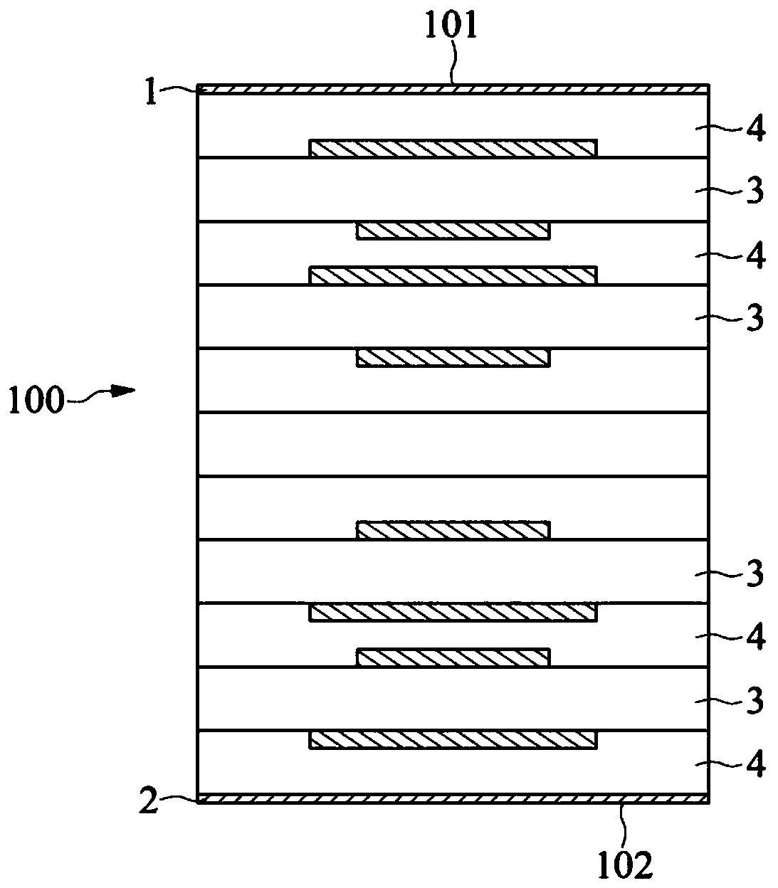
[0059] Such as figure 1 and figure 2 , step S101 is to provide a multi-layer board 100 . T...


PUM


Abstract

The invention discloses a circuit board and a manufacturing method thereof. The manufacturing method of the circuit board includes the following steps: providing a multilayer board, wherein the multilayer board has a top surface and a bottom surface; implementing a first hole drilling step to form a first through hole running through the top surface and the bottom surface of the multilayer board;implementing a through hole plating step to plate a first conductive layer on the hole wall of the first through hole; implementing a first hole plugging step to fill the first through hole with resin; and implementing a second hole drilling step: carrying out hole drilling towards the first conductive layer of the multilayer board to form two first perforations which run through the top surface and the bottom surface of the multilayer board and are distributed at intervals, wherein each first perforation partially overlaps the first through hole, and part of the first conductive layer is removed so that the first conductive layer forms two first sub conductive layers separated from each other.

Description

technical field [0001] The invention relates to a circuit board and a manufacturing method thereof, in particular to a circuit board with a multilayer board structure and a manufacturing method thereof. Background technique [0002] Generally, the part of the printed circuit board (PCB) where the ball grid array package (BGA) is designed is the area with the densest network (NET). The existing high-density interconnect (HDI) circuit board manufacturing method is realized by stacking multiple layers of laser holes. As the product design density of future printed circuit boards is getting higher and higher, the density of the network of the ball grid array package (BGA) part of the printed circuit board is also getting higher and higher. Therefore, it is increasingly difficult for the existing manufacturing methods of circuit boards to meet the requirements of the manufacturing process. Furthermore, since the multilayer stacking method of laser holes needs to be increased la...

Claims


Application Information

Patent Timeline
Patent Type & Authority Patents(China)
IPC IPC(8): H05K3/00H05K3/42H05K1/11
Inventor 赵新杨海孙奇杨伟雄
Owner TRIPOD WUXI ELECTRONICS
Why Eureka
Try Eureka