A silicon-on-insulator radio frequency switching device and its manufacturing method

A silicon-on-insulator, RF switch technology, applied in semiconductor/solid-state device manufacturing, semiconductor devices, transistors, etc., can solve problems such as inability to export PW everywhere in time, parasitic NPN potential rise, and MOSFET breakdown easily. Floating body effect, increasing breakdown voltage, reducing the effect of collection of positive charges

Active Publication Date: 2022-02-15
SHANGHAI HUAHONG GRACE SEMICON MFG CORP
View PDF7 Cites 0 Cited by
  • Summary
  • Abstract
  • Description
  • Claims
  • Application Information

AI Technical Summary

Problems solved by technology

In the top view, the monocrystalline silicon is in the shape of a "T", the source and drain electrodes are located on the vertical sides of the "T", and the body region contact device connection area is located above the horizontal of the "T". image 3 It is the state-of-the-art silicon-on-insulator RF switching device structure along the figure 1 The cross-sectional schematic diagram of the line BB', PW is the body region of the transistor, the distance from the entire body region to the body contact node P+ is relatively long, about 10 microns, therefore, there is a parasitic resistance, and when the MOSFET is turned on, it collides at the drain end The holes generated by ionization cannot be exported to PW everywhere in time, causing the potential of the base of the parasitic NPN to rise, the parasitic NPN is turned on, and the MOSFET is more prone to breakdown

Method used


Image

  • A silicon-on-insulator radio frequency switching device and its manufacturing method
  • A silicon-on-insulator radio frequency switching device and its manufacturing method
  • A silicon-on-insulator radio frequency switching device and its manufacturing method

Examples


Embodiment Construction

[0030] The specific implementation manner of the present invention will be described in more detail below with reference to schematic diagrams. Advantages and features of the present invention will be apparent from the following description and claims. It should be noted that all the drawings are in a very simplified form and use imprecise scales, and are only used to facilitate and clearly assist the purpose of illustrating the embodiments of the present invention.

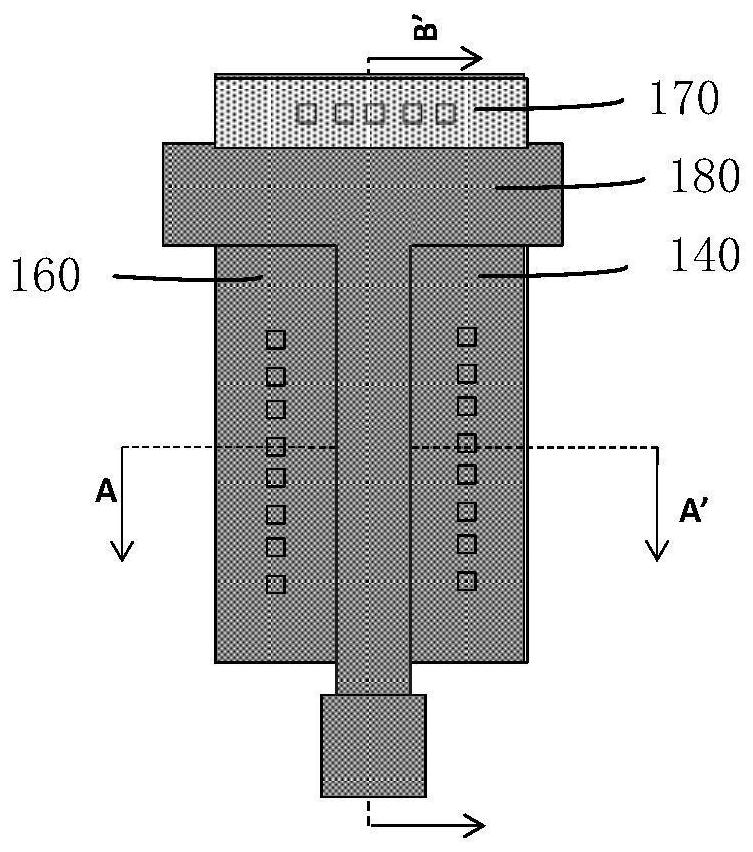
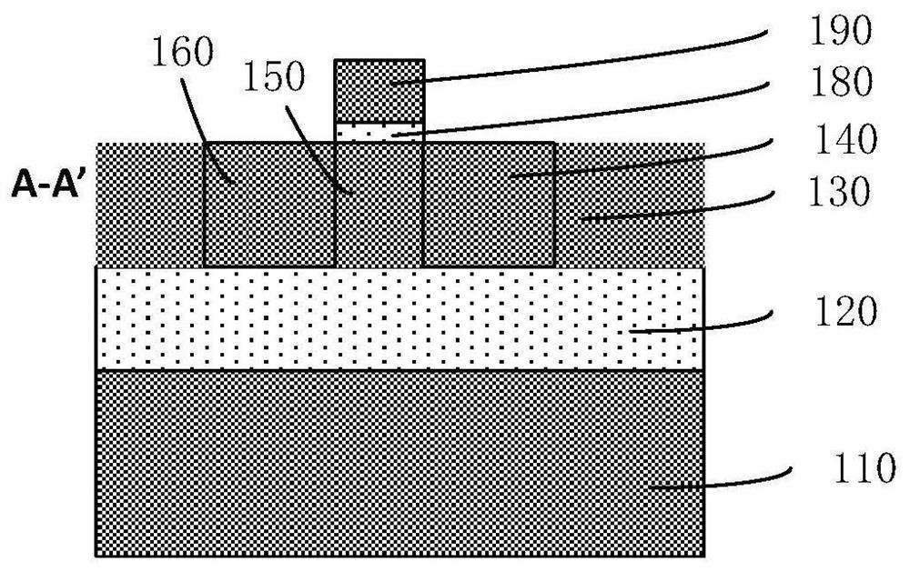
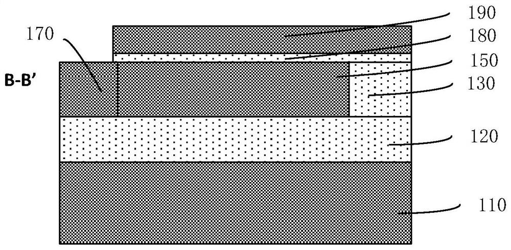
[0031] Please refer to Figure 4 , the invention provides a method for manufacturing a silicon-on-insulator radio frequency switching device, comprising:

[0032] S11: providing a substrate;

[0033] S12: sequentially forming a first oxide layer, a first single crystal silicon layer, a second oxide layer, a second single crystal silicon layer, a third oxide layer and a mask layer on the substrate;

[0034] S13: sequentially etching the mask layer, the third oxide layer, the second single crystal silicon layer,...


PUM


Abstract

The invention provides a silicon-on-insulator radio frequency switching device and a manufacturing method thereof, comprising: forming a first oxide layer, a first single-crystal silicon layer, a second oxide layer, a second single-crystal silicon layer, The third oxide layer and the mask layer; the first opening and the second opening are formed by etching the mask layer, the third oxide layer, the second single crystal silicon layer and the second oxide layer; Epitaxial growth in the opening makes it consistent with the surface of the second single crystal silicon layer; etching mask layer, third oxide layer, second single crystal silicon layer, second oxide layer and first single crystal silicon layer are formed The first trench, the second trench and the third trench; deposit plasma oxide into the three trenches to form a shallow trench isolation structure; remove the third oxide layer and the mask layer; Body contact devices are formed on the two monocrystalline silicon layers. Compared with the prior art, the parasitic capacitance and the collection of positrons can be reduced, the floating body effect is suppressed, and the breakdown voltage is improved at the same time.

Description

technical field [0001] The invention relates to the technical field of semiconductors, in particular to a silicon-on-insulator radio frequency switching device and a manufacturing method thereof. Background technique [0002] Silicon is the most widely used primary raw material in the semiconductor industry, and most chips are made of silicon wafers. Silicon-on-insulator (SOI) is a special silicon chip whose main feature is to insert an insulating layer (buried oxide layer) between the active layer and the substrate layer to isolate the electrical connection between the active layer and the substrate. Connection, this structural feature brings many advantages such as small parasitic effect, fast speed, low power consumption, high integration, and strong radiation resistance to silicon-on-insulator devices. [0003] In the existing technology, such as Figure 1 to Figure 3 , figure 1 is a top view of a silicon-on-insulator RF switching device structure in the prior art, ...

Claims


Application Information

Patent Timeline
Patent Type & Authority Patents(China)
IPC IPC(8): H01L21/336H01L29/786H01L29/06
Inventor 刘张李
Owner SHANGHAI HUAHONG GRACE SEMICON MFG CORP
Why Eureka
Try Eureka