Array substrate and preparation method thereof
An array substrate and substrate technology, which is applied to electrical components, electrical solid-state devices, circuits, etc., can solve problems such as the inability to release charge accumulation and affecting the yield of array substrate products.
- Summary
- Abstract
- Description
- Claims
- Application Information
AI Technical Summary
Problems solved by technology
Method used
Image

Examples
Embodiment 1
[0054] Such as Figure 1 to Figure 6 As shown, this embodiment provides a method for manufacturing an array substrate, including: forming a multi-layer conductive layer on the substrate.
[0055] Wherein, the step of forming each conductive layer may include: forming a pattern including a conductive pattern and an antistatic pattern through a patterning process, the conductive pattern is electrically connected to the antistatic pattern, and the antistatic patterns in different layers are electrically connected.
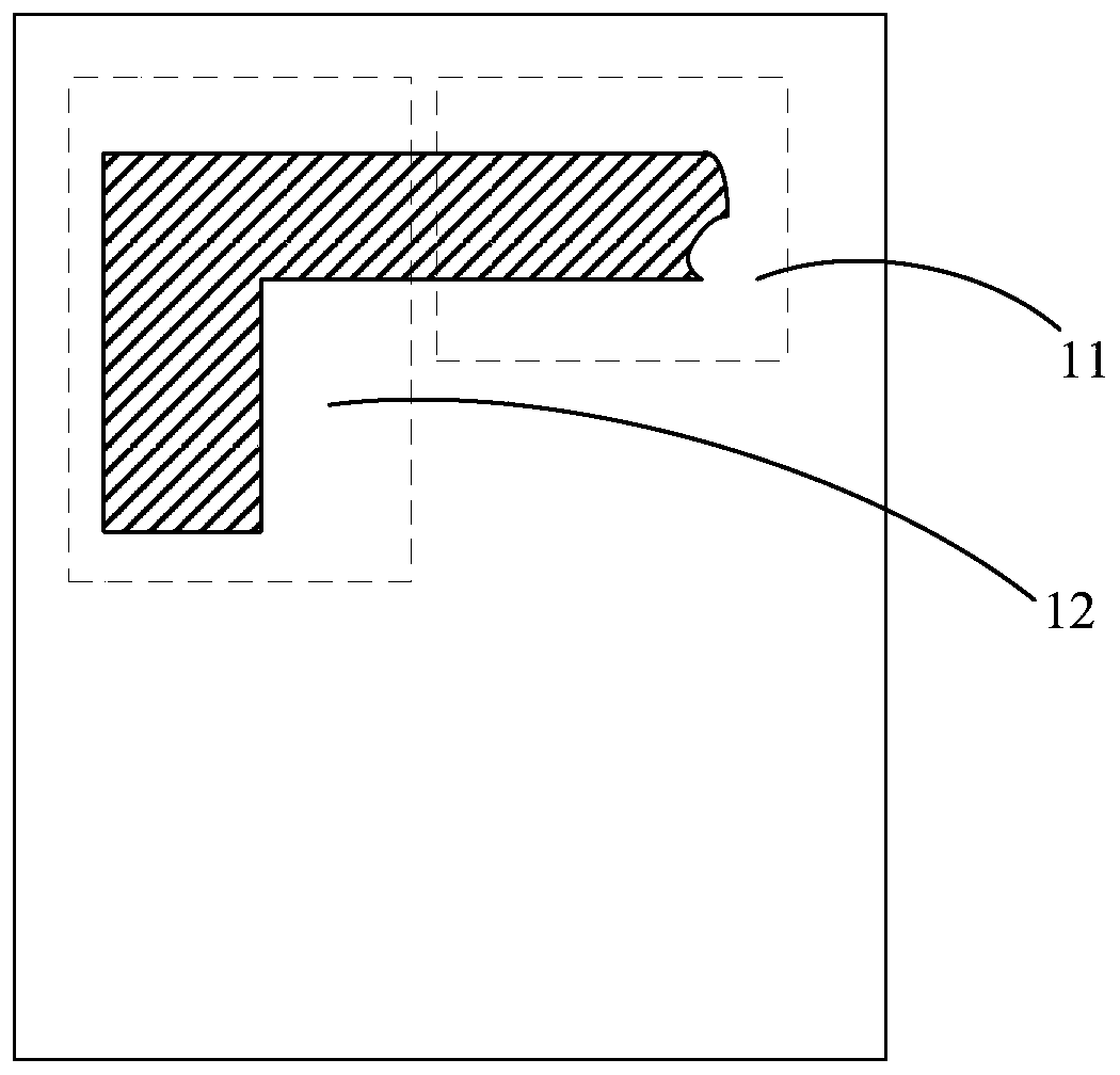
[0056] That is, in this embodiment, each conductive layer includes a conductive pattern and an antistatic pattern. Wherein, the conductive patterns in different conductive layers may respectively be gates, sources, drains, pixel electrodes, common electrodes and other structures of thin film transistors.
[0057] In this embodiment, when preparing the array substrate, the conductive patterns in the same conductive layer are electrically connected to the antistatic pa...
Embodiment 2
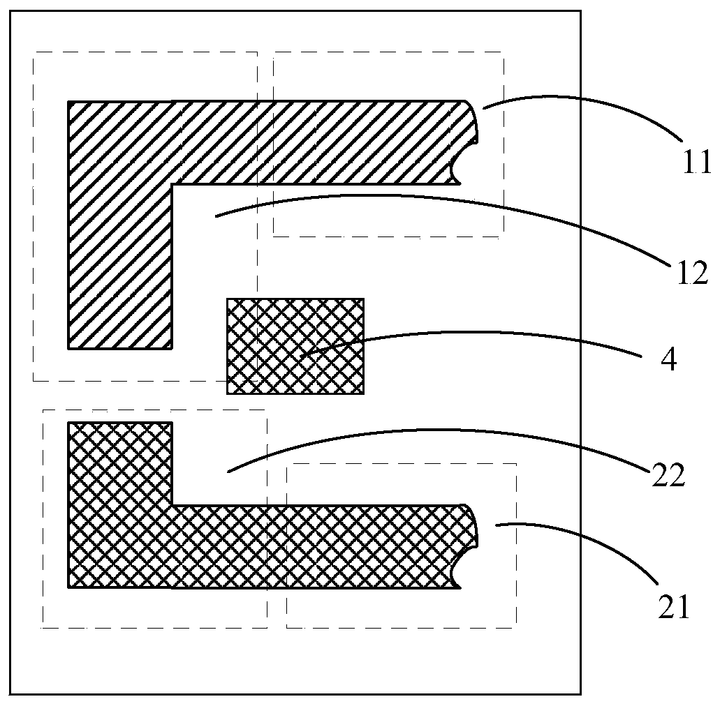
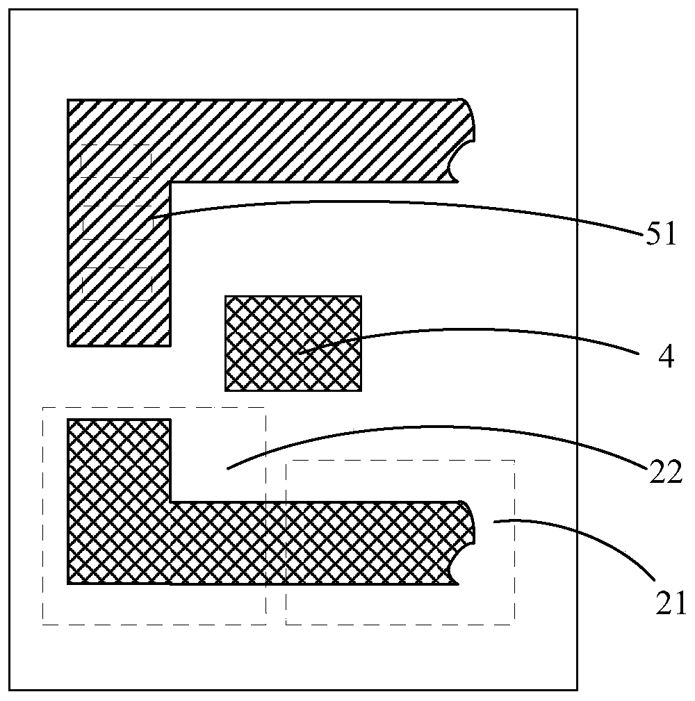
[0092] Such as Figure 7-12 As shown, this embodiment provides a method for preparing an array substrate, which is basically the same as the method for preparing the array substrate provided in Embodiment 1.
[0093] Particularly, in this embodiment, at least part of the conductive layer of the array substrate includes a plurality of conductive patterns, and the plurality of conductive patterns are electrically connected to the antistatic pattern in the same conductive layer. Specifically, in this embodiment, the first conductive layer includes a plurality of first conductive patterns 11, and the first conductive pattern 11 is a gate, and the third conductive layer includes a plurality of third conductive patterns 31, and the third conductive pattern The pattern 31 will be described as an example of a source and a drain.
[0094] The preparation method of the present embodiment also includes the following steps on the basis of Example 1:
[0095] S21, such as Figure 6 As s...
Embodiment 3
[0117] This embodiment provides an array substrate, which can be prepared according to the preparation method provided in Embodiment 1 or Embodiment 2. The array substrate includes: a base and multiple conductive layers arranged on the base; each conductive layer includes a conductive pattern and an antistatic pattern, and the conductive pattern is electrically connected to the antistatic pattern; the antistatic patterns in different layers are electrically connected.
[0118] Since the array substrate provided in this embodiment is not prone to electrostatic discharge during the preparation process, the array substrate has a higher yield rate and better performance.
PUM
 Abstract
Description
Claims
Application Information
 - R&D
- Intellectual Property
- Life Sciences
- Materials
- Tech Scout
- Unparalleled Data Quality
- Higher Quality Content
- 60% Fewer Hallucinations
Browse by: Latest US Patents, China's latest patents, Technical Efficacy Thesaurus, Application Domain, Technology Topic, Popular Technical Reports.
© 2025 PatSnap. All rights reserved.Legal|Privacy policy|Modern Slavery Act Transparency Statement|Sitemap|About US| Contact US: help@patsnap.com