A display substrate, its preparation method, and a display panel
A display substrate and display panel technology, which is applied in semiconductor/solid-state device manufacturing, diodes, semiconductor devices, etc., can solve problems such as color shift, serious color shift, pixel color deviation, etc., to reduce color shift, pure color, and reduce color The effect of deviation
- Summary
- Abstract
- Description
- Claims
- Application Information
AI Technical Summary
Problems solved by technology
Method used
Image
Examples
no. 1 example
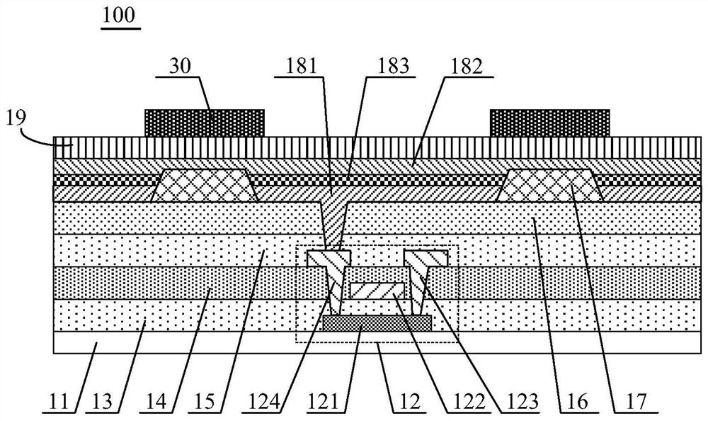
[0055] image 3 A schematic structural diagram of a substrate is shown for an embodiment of the present invention. Such as image 3 As shown, the display substrate 100 includes a base 11 and a plurality of OLED devices 18 disposed on the base 11 . The display substrate 100 also includes a thin film encapsulation layer 19 and a light blocking layer 30 . The thin film encapsulation layer 19 is disposed on the OLED device 18, the light blocking layer 30 is disposed on the thin film encapsulation layer 19, and the light blocking layer 30 is located between two adjacent OLED devices 18, the light blocking layer 30 can block light from passing through.
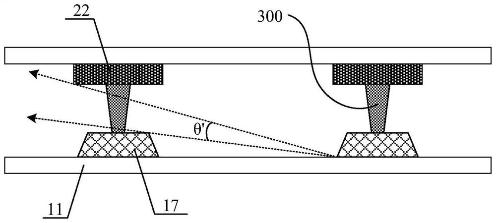
[0056] Figure 4 to include image 3 The schematic diagram of the structure of the display panel of the display substrate is shown. Figure 5 for Figure 4 A simplified schematic diagram of the light emitting direction of the OLED device of the shown display panel. The display panel includes a display substrate 100 and a cove...
no. 2 example
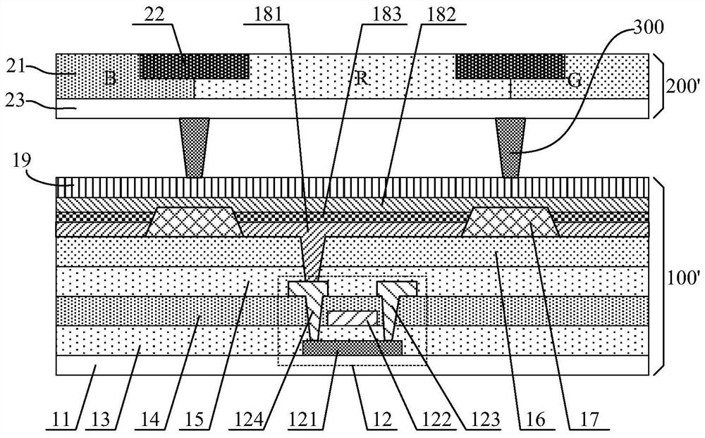
[0082] Based on the inventive concepts of the foregoing embodiments, the embodiments of the present invention further provide a display panel. Such as Figure 4 As shown, the display panel includes the display substrate 100 in the above embodiments, and also includes a cover plate 200 . The cover plate 200 and the display substrate 100 are arranged in opposition, and an isolation column 300 is disposed between the cover plate 200 and the display substrate 100 . The cover plate 200 includes a second base (not shown in the figure), and a color filter layer 21 disposed on a side of the second base facing the display substrate. The color filter layer 21 includes a red color filter (R), a green color filter (G) and a blue color filter (B) corresponding to the light-emitting areas, so as to form pixels corresponding to the light-emitting areas on the display panel. The red pixels are located on the red color film (R), the green pixels are located on the green color film (G), and t...
PUM
| Property | Measurement | Unit |
|---|---|---|
| thickness | aaaaa | aaaaa |
Abstract
Description
Claims
Application Information
 - R&D
- Intellectual Property
- Life Sciences
- Materials
- Tech Scout
- Unparalleled Data Quality
- Higher Quality Content
- 60% Fewer Hallucinations
Browse by: Latest US Patents, China's latest patents, Technical Efficacy Thesaurus, Application Domain, Technology Topic, Popular Technical Reports.
© 2025 PatSnap. All rights reserved.Legal|Privacy policy|Modern Slavery Act Transparency Statement|Sitemap|About US| Contact US: help@patsnap.com


