Patching method and device

A patch and sheet technology, which is applied in the direction of assembling printed circuits with electrical components, electrical components, and printed circuit manufacturing, etc., can solve the problems of difficult to guarantee the quality of the placement and difficult to accurately position the placement head, so as to ensure the quality and adapt to the The effect of strong performance and accurate printing position

Active Publication Date: 2019-04-02
惠州市协昌电子有限公司
View PDF8 Cites 7 Cited by
  • Summary
  • Abstract
  • Description
  • Claims
  • Application Information

AI Technical Summary

Problems solved by technology

For example, in LED products, according to different application scenarios, the shape of the lamp panel is different, and the LED lamp beads may be arranged in a circle or an irregular curve. When this type of structure

Method used


Image

  • Patching method and device
  • Patching method and device
  • Patching method and device

Examples


Embodiment Construction

[0032] In order to facilitate those skilled in the art to understand the present invention, the present invention will be further described in detail below in conjunction with specific embodiments and accompanying drawings.

[0033] A patch method and device provided by the present invention comprise the following steps:

[0034] Step 1, screening chip components, and screening out unqualified chip components;

[0035] Step 2: Select the corresponding component tray according to the shape and size of the chip components, and place the chip components neatly on the component tray;

[0036] Step 3, according to the position of the patch on the circuit board, make a solder paste positioner with the same size as the circuit board for auxiliary printing of solder paste;

[0037] Step 4, cover the positioning part on the circuit board, and print solder paste on the patch position;

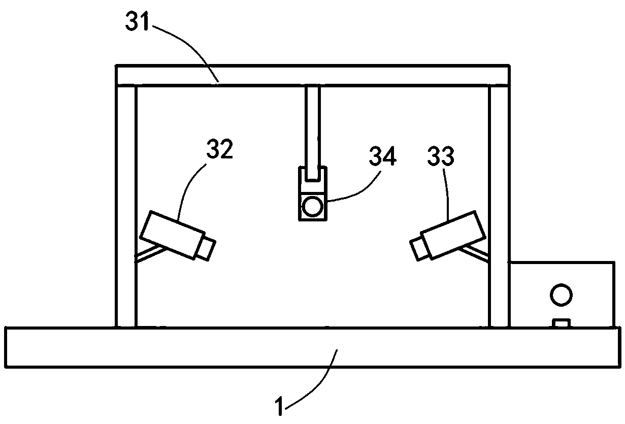
[0038] Step 5, put the circuit board printed with solder paste on the circuit board fixing jig of t...


PUM

PropertyMeasurementUnit
Thicknessaaaaaaaaaa

Abstract

The invention relates to a patching method and device. According to the patching method and device, circuit board printing solder paste is assisted by adoption of a positioning member; and when patching is carried out, an image of a circuit board is acquired through a visual acquisition mechanism to calculate an accurate coordinate and judge whether a patching position is correct or not. The patching device comprises a machine platform, a circuit board fixing jig, a visual detection mechanism, a patching mechanism and a circuit board positioning jig, wherein the circuit board fixing jig is arranged on the machine platform and is used for placing the circuit board; the visual detection mechanism is arranged on one side of the machine platform and is used for detecting the circuit board; thepatching mechanism is arranged on the other side of the machine platform and is used for patching the circuit board; and the circuit board positioning jig is located between the patching mechanism and the visual detection mechanism. According to the patching method and device, repeated coordinate acquisition comparison and detection are carried out in the patching process, so that the correctnessof the patching position is ensured, the product quality if ensured, the patching of small components and components complicated in arrangement is satisfied, and the adaptability is relatively strong.

Description

technical field [0001] The invention relates to the technical field of PCB patch processing, in particular to a patch method and device. Background technique [0002] PCB (Printed Circuit Board), the Chinese name is printed circuit board, also known as printed circuit board, is an important electronic component, a support for electronic components, and a carrier for electrical connections of electronic components. SMT (Surface Mounted Technology) is the surface mount technology, which is the most popular technology and process in the electronic assembly industry. Devices) are mounted on the surface of the PCB or the surface of other substrates, and are soldered and assembled by reflow soldering or dip soldering. With the continuous development and progress of technology, all kinds of electronic components are becoming more and more refined, and they are constantly developing towards miniaturization, and the requirements for placement are also getting higher and higher. For...

Claims


Application Information

Patent Timeline
IPC IPC(8): H05K3/34H05K13/00H05K13/04
CPCH05K3/341H05K13/0015H05K13/0465
Inventor 袁延辉袁楷焯袁宏斌李荣梅
Owner 惠州市协昌电子有限公司
Why Eureka
Try Eureka