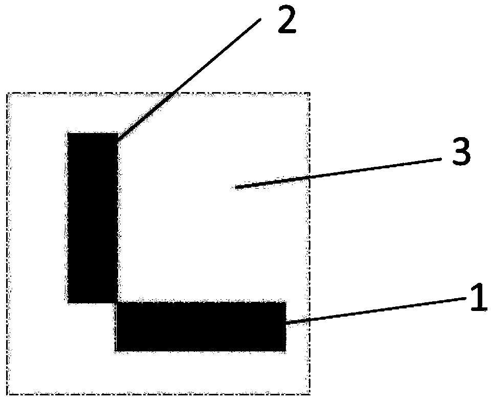
Preparation method of double-layer chiral structure
A chiral structure, double-layer technology, applied in optical components, instruments, optics, etc., can solve the complicated and complicated problems of double-layer chiral metal micro-nano structures, achieve the effect of simple and easy to operate in the preparation process, and avoid operational errors
- Summary
- Abstract
- Description
- Claims
- Application Information
AI Technical Summary
Problems solved by technology
Method used
Image
Examples
Embodiment 1
[0037] A method for preparing a double-layer chiral structure, comprising the following steps:
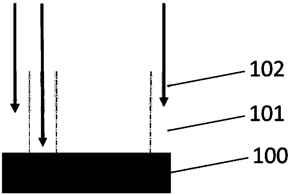
[0038] Step 1: Prepare the glass substrate 100, prepare the ITO glass substrate 100 and clean it for use;
[0039] in particular:
[0040] Prepare an ITO glass substrate 100 with a thickness of 1.0mm and a length and width of 20.0mm*20.0mm, and put the prepared ITO glass into a washing solution to clean it. After ultrasonication with deionized water for 15 minutes, ultrasonication with acetone for 15 minutes, and alcohol Sonicate for 15 minutes, then use deionized water to sonicate for 5 minutes, and finally dry it with a nitrogen gun and put it in a nitrogen cabinet for later use.
[0041] Step 2: Coating photoresist on the substrate 100, and throwing two photoresist layers on the surface of the substrate 100 with a glue-spinning machine;
[0042] in particular:
[0043] The specific steps of removing glue are as follows: on the prepared glass substrate 100, use a glue removing...
Embodiment 2
[0057] For the double-layer chiral structure prepared in this embodiment, only the thickness of the metal material 103 vertically evaporated by the electron beam evaporation coating apparatus is changed, and the preparation process is the same as that in Embodiment 1.
[0058] in particular:
[0059] When using the electron beam vacuum evaporation coating instrument to vertically evaporate the metal material 103, the thickness of the evaporated metal material 103 is controlled, and the thickness of the electron beam evaporation coating instrument to vertically evaporate the metal material 103 is less than the thickness of the positive glue 101, such as Figure 8 shown. After the coating is evaporated, the photoresist stripping process is performed, and the substrate 100 is soaked with a negative stripping solution to dissolve the negative glue 102, and the soaking time is at least 30 minutes. like Figure 9 As shown, after the negative resist 102 is removed, the metal materi...
PUM
 Abstract
Description
Claims
Application Information
 - R&D
- Intellectual Property
- Life Sciences
- Materials
- Tech Scout
- Unparalleled Data Quality
- Higher Quality Content
- 60% Fewer Hallucinations
Browse by: Latest US Patents, China's latest patents, Technical Efficacy Thesaurus, Application Domain, Technology Topic, Popular Technical Reports.
© 2025 PatSnap. All rights reserved.Legal|Privacy policy|Modern Slavery Act Transparency Statement|Sitemap|About US| Contact US: help@patsnap.com


