


Quick Research
Generate reliable direction feasibility study reports for your R&D in just a few steps.

Technical Q&A
Discover and master advanced knowledge NOW. Basics, ideas, possibilities, all at once.

Find Solutions
As an expert in R&D theories, this can generate solutions to your technical problems instantly.

Evaluate Feasibility
Analyze your overall solution with one click, know your potential R&D risks in advance.

Monitor Landscape
Get weekly tech updates, stay abreast of the latest tech innovations and key insights.
Semiconductor device
A technology for semiconductors and devices, applied in the field of semiconductor devices, can solve the problems of low heat dissipation of insulating paste and reduced driveability of small spheres, and achieve the effect of improving heat dissipation
- Summary
- Abstract
- Description
- Claims
- Application Information
AI Technical Summary
Problems solved by technology
Method used
Image

Examples
no. 1 approach
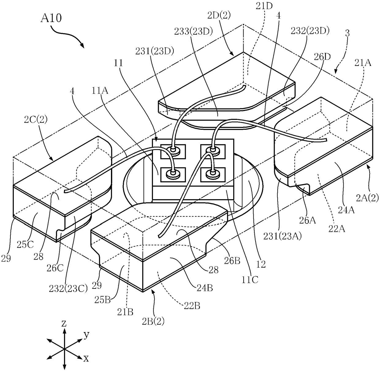
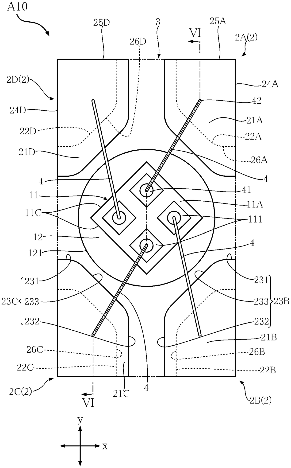
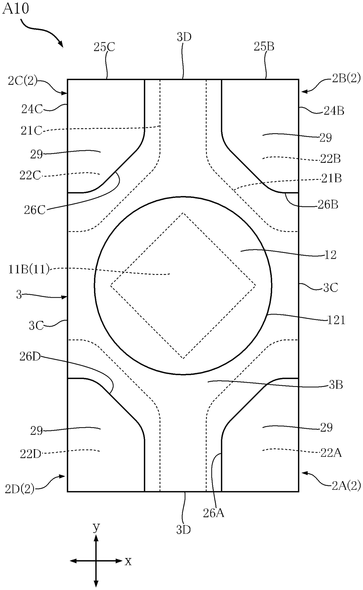
[0145] according to Figure 1 to Figure 7 , the semiconductor device A10 according to the first embodiment of the present invention will be described. The semiconductor device A10 includes a semiconductor element 11 , a conductive layer 12 , a plurality of terminals 2 , a sealing resin 3 and a plurality of wires 4 .
[0146] exist figure 1 In , the sealing resin 3 is shown transparently for easy understanding. exist figure 2 In FIG. 2 , the internal conductive layer 28 (details will be described later) and the sealing resin 3 are shown transparently for easy understanding. exist figure 1 and figure 2 In , the external shape of the sealing resin 3 seen through is shown by a phantom line (two-dot chain line). represented by a dotted line figure 2 The passage position of the VI-VI line shown. Figure 8 The section position of Image 6 The location of the section is the same. In addition, in Figure 1 to Figure 7 In the illustrated plurality of terminals 2 , descript...
no. 2 approach
[0189] Below, according to Figure 19 ~ Figure 23 , the semiconductor device A20 according to the second embodiment of the present invention will be described. In these figures, the same reference numerals are assigned to the same or similar components as those of the semiconductor device A10 described above, and overlapping descriptions will be omitted. Here, for ease of understanding, in Figure 19 In , the inner conductive layer 28 and the sealing resin 3 are shown transparently. exist Figure 19 In , the external shape of the sealing resin 3 seen through is shown by a phantom line. represented by a dotted line Figure 19 The passing position of line XXIII-XXIII shown. In addition, in figure 1 9~ Figure 23 In , the reference numerals of the same constituent elements that overlap are omitted for the plurality of terminals 2 .
[0190] The structures of the plurality of terminals 2 and the sealing resin 3 of the semiconductor device A20 are different from those of t...
no. 3 approach
[0196] according to Figure 24 ~ Figure 26 , the semiconductor device A30 according to the third embodiment of the present invention will be described. In these figures, the same reference numerals are assigned to the same or similar components as those of the semiconductor device A10 described above, and overlapping descriptions will be omitted. Here, for ease of understanding, in Figure 24 In , the inner conductive layer 28 and the sealing resin 3 are shown transparently. exist Figure 24 In , the external shape of the sealing resin 3 seen through is shown by a phantom line. Figure 26 is an enlarged cross-sectional view of the semiconductor device A30, and its cross-sectional position is the same as Figure 7 The location of the section is the same. In addition, in Figure 24 and Figure 25 In , the reference numerals of the same constituent elements that overlap are omitted for the plurality of terminals 2 .
[0197] The structure of the conductive layer 12 of the...
PUM
 Abstract
Description
Claims
Application Information
 - R&D Engineer
- R&D Manager
- IP Professional
- Industry Leading Data Capabilities
- Powerful AI technology
- Patent DNA Extraction
Browse by: Latest US Patents, China's latest patents, Technical Efficacy Thesaurus, Application Domain, Technology Topic, Popular Technical Reports.
© 2024 PatSnap. All rights reserved.Legal|Privacy policy|Modern Slavery Act Transparency Statement|Sitemap|About US| Contact US: help@patsnap.com