
3D memory device and manufacturing method thereof

A memory device, 3D technology, applied in the field of memory, can solve problems such as occupying a large space of 3D memory devices, difficulty in controlling wafer warpage, complex process, etc., to improve yield and reliability, reduce depth differences, and reduce manufacturing costs. cost effect

Active Publication Date: 2020-11-13
YANGTZE MEMORY TECH CO LTD
View PDF4 Cites 0 Cited by
  • Summary
  • Abstract
  • Description
  • Claims
  • Application Information

AI Technical Summary

Problems solved by technology

However, in a 3D memory device, the conductive channel only supplies power to the channel pillars on both sides of it, so it is necessary to form a plurality of gate line spacers first, and then fill the gate line spacers to form a conductive channel after forming the channel columns. The process is complicated, and the conductive channel needs to occupy a large amount of space in the 3D memory device. In addition, because the conductive channel needs to fill the entire gate line spacer, not only is it difficult to control the warpage of the wafer, but also more consumables and higher costs

Method used


Image

  • 3D memory device and manufacturing method thereof
  • 3D memory device and manufacturing method thereof
  • 3D memory device and manufacturing method thereof

Examples


Embodiment Construction

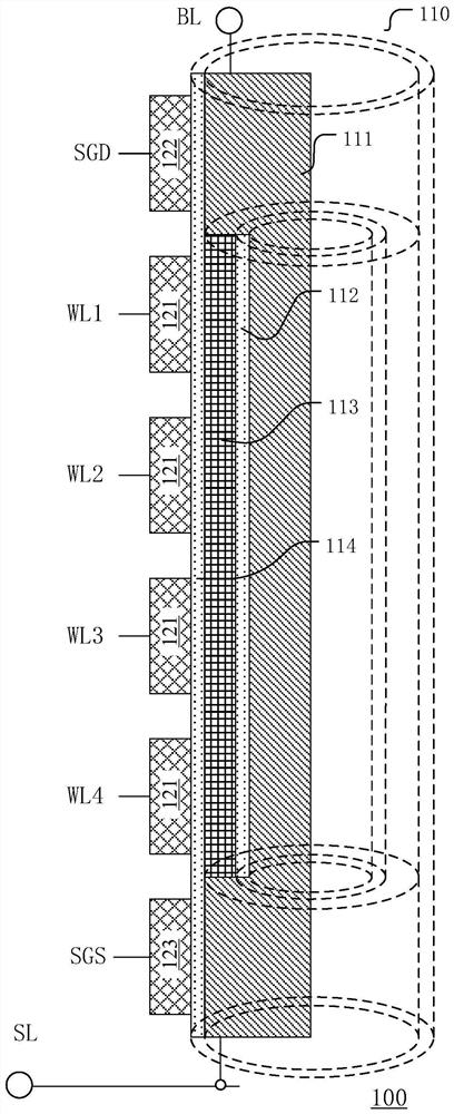
[0033] Hereinafter, the present invention will be described in more detail with reference to the accompanying drawings. In the various figures, identical elements are indicated with similar reference numerals. For the sake of clarity, various parts in the drawings have not been drawn to scale. Also, some well-known parts may not be shown. For the sake of simplicity, the semiconductor structure obtained after several steps can be described in one figure.

[0034] It should be understood that when describing the structure of a device, when a layer or a region is referred to as being "on" or "over" another layer or another region, it may mean being directly on another layer or another region, or Other layers or regions are also included between it and another layer or another region. And, if the device is turned over, the layer, one region, will be "below" or "beneath" the other layer, another region.

[0035] If it is to describe the situation directly on another layer or an...


PUM


Abstract

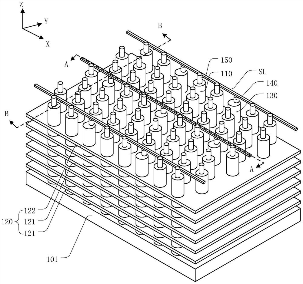
The application discloses a 3D storage device and a manufacturing method thereof. The 3D memory device includes: a semiconductor substrate; a gate stack structure located on the semiconductor substrate, including a plurality of alternately stacked gate conductors and a plurality of interlayer insulating layers; and a plurality of channel columns passing through the gate stack structure , and is electrically connected to the semiconductor substrate; the 3D memory device also includes a conductive column, which runs through the gate stack structure, is electrically connected to the semiconductor substrate, and is distributed between a plurality of channel columns, and each conductive column is used to pass through the semiconductor substrate. The bottom supplies power to the surrounding channel posts.

Description

technical field [0001] The present invention relates to memory technology, and more specifically, to a 3D memory device and a manufacturing method thereof. Background technique [0002] The improvement of the storage density of the memory device is closely related to the progress of the semiconductor manufacturing process. As the feature size of the semiconductor manufacturing process becomes smaller and smaller, the storage density of the memory device becomes higher and higher. In order to further increase storage density, memory devices with a three-dimensional structure (ie, 3D memory devices) have been developed. A 3D memory device includes a plurality of memory cells stacked in a vertical direction, which can double the integration level on a wafer per unit area and reduce the cost. [0003] Existing 3D memory devices are mainly used as non-volatile flash memory. The two main non-volatile flash memory technologies use NAND and NOR structures, respectively. Compared...

Claims


Application Information

Patent Timeline
Patent Type & Authority Patents(China)
IPC IPC(8): H01L27/11582H10B43/27
CPCH10B43/27
Inventor 华文宇刘藩东
Owner YANGTZE MEMORY TECH CO LTD
Learn More