Direct-inserting type silicon wafer inserting and extracting device

A silicon chip insertion and component technology, which is applied in transportation and packaging, electrical components, semiconductor/solid-state device manufacturing, etc., can solve problems such as silicon chip damage, silicon chip damage, and complex structure

Pending Publication Date: 2019-02-15
ROBOTECHN INTELLIGENT TECH CO LTD
View PDF0 Cites 4 Cited by
  • Summary
  • Abstract
  • Description
  • Claims
  • Application Information

AI Technical Summary

Problems solved by technology

Among them, because the thickness of the silicon wafer is very thin and the material is relatively brittle, the clamping type is easy to cause damage to the silicon wafer. The structure of the electromagnetic adsorption type and the vacuum adsorption type are more complicated, and the parts are more difficult to process. At the center position, at the moment of vacuum pumping and inflating, the gas will cause a large local impact on the silicon wafer, and in order to obtain sufficient adsorption force, the contact area between the suction cup and the silicon wafer is often reduced, so that the formed vacuum adsorption chamber is concentrated At the center of the suction cup, this will cause the center of the silicon wafer to be concentrated and cause damage to the silicon wafer

Method used


Image

  • Direct-inserting type silicon wafer inserting and extracting device
  • Direct-inserting type silicon wafer inserting and extracting device
  • Direct-inserting type silicon wafer inserting and extracting device

Examples


Embodiment Construction

[0027] The present invention will be further described below with reference to the accompanying drawings and specific embodiments, so that those skilled in the art can better understand and implement the present invention, but the examples cited are not intended to limit the present invention.

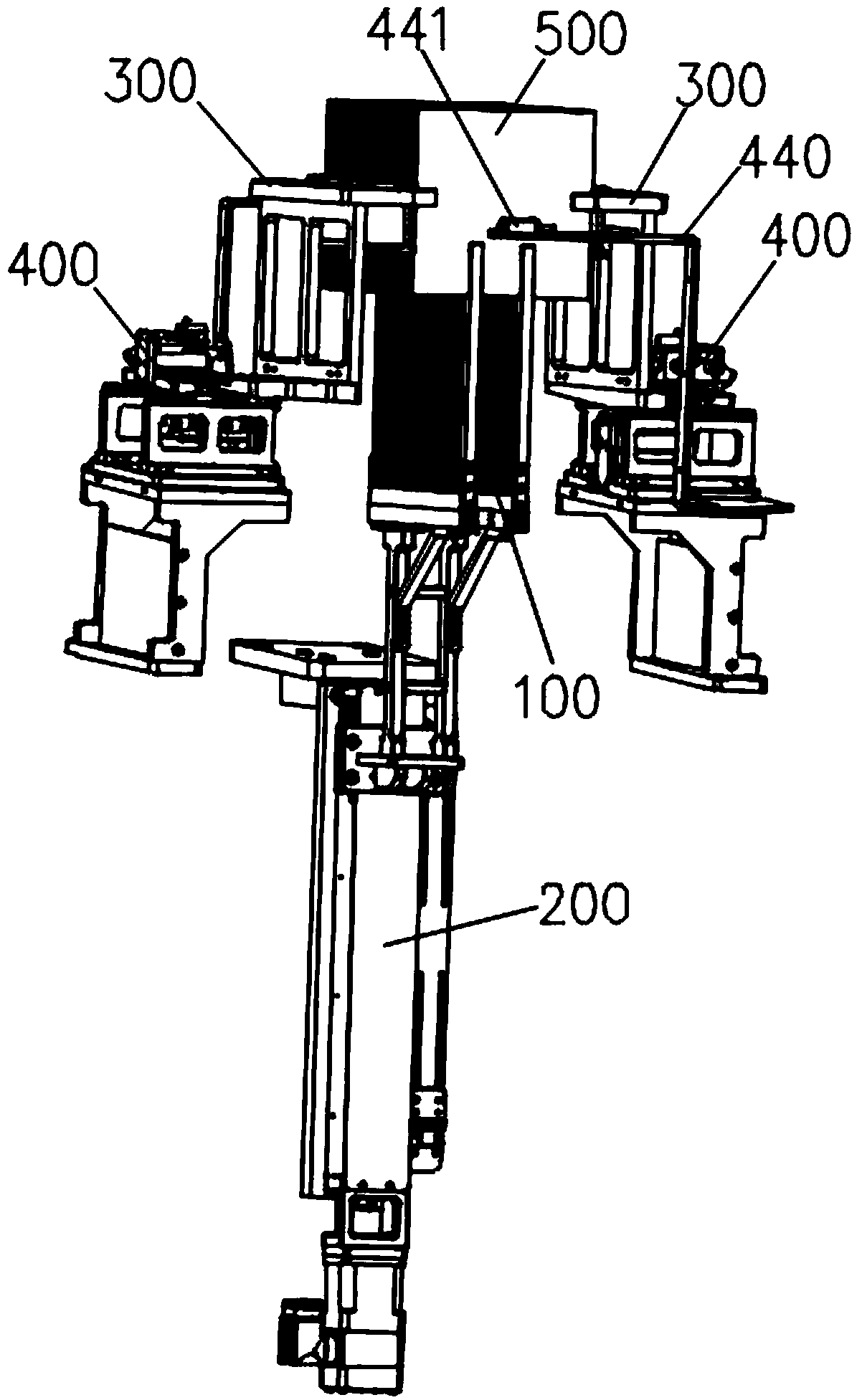
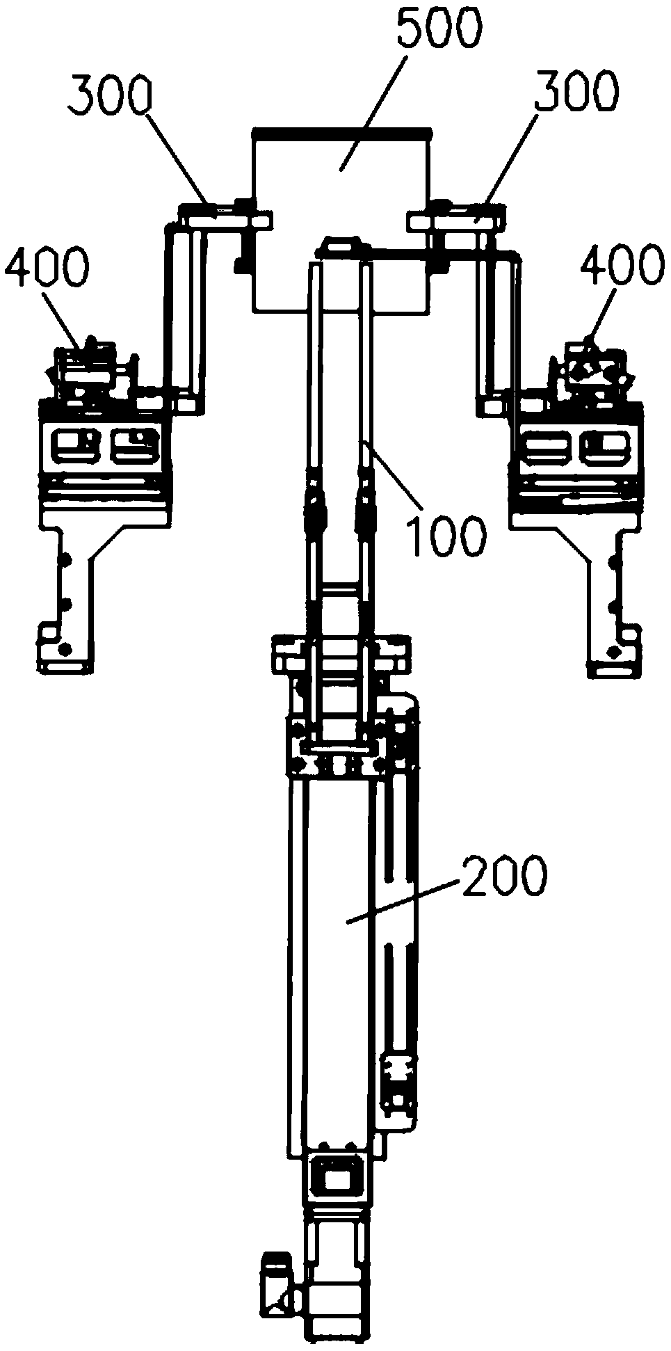
[0028] Such as Figure 1-7 As shown, the in-line silicon wafer inserting and picking device in this embodiment includes a comb tooth assembly 100, a lifting drive assembly 200, a two-center assembly 300, and a horizontal drive assembly 400.

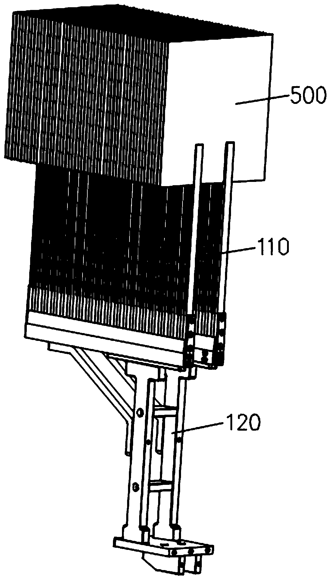
[0029] Such as Figure 3-4 As shown, the comb tooth assembly 100 includes two sets of comb teeth 110 that are parallel to each other and arranged at intervals. The comb teeth 110 include a number of comb teeth 111 arranged in sequence. Interval grooves 112 are provided between adjacent comb teeth 111. A clamping groove 113 is provided on the top of 111, and the clamping groove 113 is used for clamping the product. In this embodiment, the depth of the s...


PUM


Abstract

The invention relates to the technical field of automatic equipment, and discloses a direct-inserting type silicon wafer inserting and extracting device. The device comprises a comb tooth assembly, alifting driving assembly, two centering assemblies and a horizontal driving assembly; the comb tooth assembly comprises two sets of comb teeth which are parallel to each other and are arranged at intervals; each comb tooth comprises a plurality of comb tooth pieces arranged in sequence; a spacing groove is formed between every two adjacent comb tooth pieces; a clamping groove is formed in the topof each comb tooth piece; the clamping grooves are used for clamping a product; the lifting driving assembly is used for driving the comb teeth to ascend and descend; the two centering assemblies arearranged on the two sides of the comb tooth assembly respectively; each centering assembly comprises a centering plate; and the horizontal driving assembly is used for driving the two centering platesto move from the two sides to the middle, thereby centering the product. Silicon wafers are centered and arranged in order, so that the silicon wafers can be conveniently inserted; and wafer inserting and extracting are carried out in a supporting and clamping mode, so that the damage rate in a silicon wafer transferring process is reduced, and meanwhile the production efficiency is improved.

Description

Technical field [0001] The invention relates to the technical field of silicon wafer production equipment, in particular to a direct-insertion type silicon wafer insertion chip taking device. Background technique [0002] In the solar silicon wafer processing steps, it is necessary to insert wafers first, that is, place multiple wafers on a quartz boat at intervals, and then perform processing, and then perform the wafer removal operation, that is, the processed silicon The piece is taken out of the quartz boat for subsequent process operations. At present, three kinds of grasping methods are mainly used to grasp silicon wafers, namely: clamping type, electromagnetic adsorption type, and vacuum chuck type. Among them, because the thickness of the silicon wafer is very thin, the material is relatively brittle, the clamping type is easy to cause damage to the silicon wafer, the electromagnetic adsorption type and the vacuum adsorption type are more complicated in structure, and th...

Claims


Application Information

Patent Timeline
IPC IPC(8): H01L21/677H01L21/687
CPCH01L21/67742H01L21/67766H01L21/67781H01L21/68707
Inventor 张学强戴军张建伟罗银兵
Owner ROBOTECHN INTELLIGENT TECH CO LTD
Why Eureka
Try Eureka