Organic electroluminescent display panel and preparation method thereof
An electroluminescent display and display panel technology, which is applied in the direction of circuits, electrical components, and electrical solid devices, can solve the problems of low material utilization rate, poor uniformity of luminescent film, and high material utilization rate of inkjet printing technology.
- Summary
- Abstract
- Description
- Claims
- Application Information
AI Technical Summary
Problems solved by technology
Method used
Image

Examples
Embodiment Construction
[0030] The following will clearly and completely describe the technical solutions in the embodiments of the present invention with reference to the accompanying drawings in the embodiments of the present invention. Obviously, the described embodiments are only some, not all, embodiments of the present invention. Based on the embodiments of the present invention, all other embodiments obtained by persons of ordinary skill in the art without making creative efforts belong to the protection scope of the present invention.
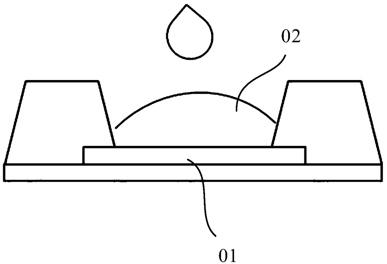
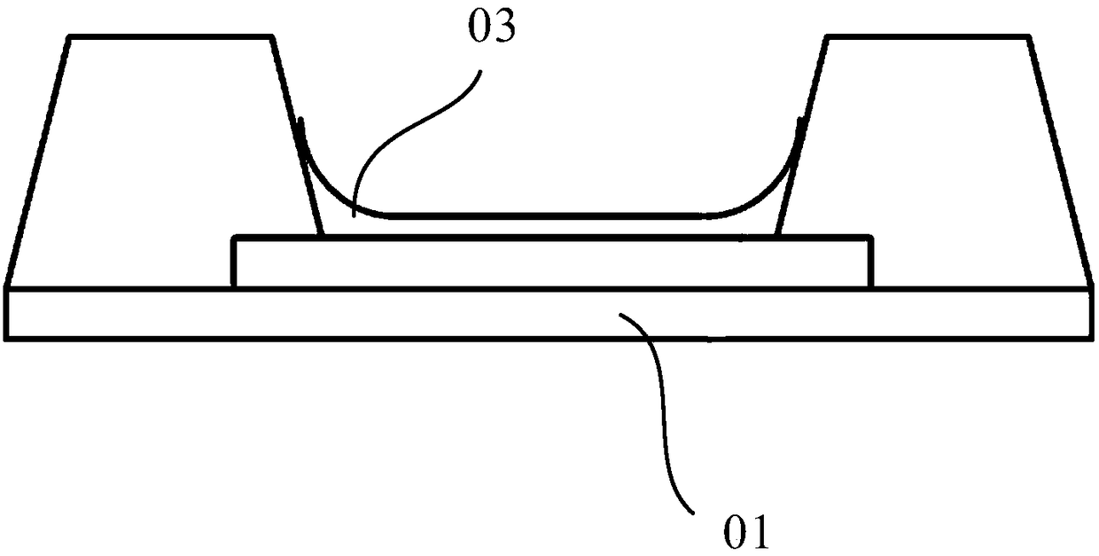
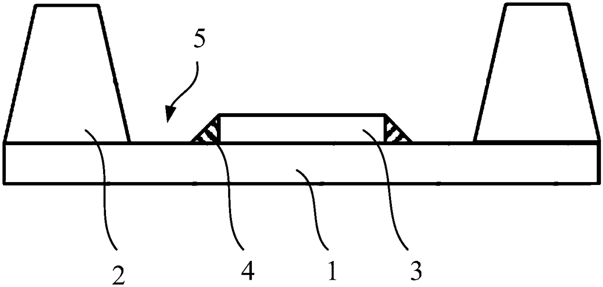
[0031] Please refer to Figure 3 to Figure 6 An organic electroluminescent display panel provided by an embodiment of the present invention includes: a base substrate 1, a pixel definition layer 2 is provided on one side of the base substrate 1, and the pixel definition layer 2 has a plurality of openings, each opening The bottom is provided with a first electrode layer 3, the projected area of the first electrode layer 3 on the base substrate 1 is smaller t...
PUM
 Abstract
Description
Claims
Application Information
 - Generate Ideas
- Intellectual Property
- Life Sciences
- Materials
- Tech Scout
- Unparalleled Data Quality
- Higher Quality Content
- 60% Fewer Hallucinations
Browse by: Latest US Patents, China's latest patents, Technical Efficacy Thesaurus, Application Domain, Technology Topic, Popular Technical Reports.
© 2025 PatSnap. All rights reserved.Legal|Privacy policy|Modern Slavery Act Transparency Statement|Sitemap|About US| Contact US: help@patsnap.com