


Quick Research
Generate reliable direction feasibility study reports for your R&D in just a few steps.

Technical Q&A
Discover and master advanced knowledge NOW. Basics, ideas, possibilities, all at once.

Find Solutions
As an expert in R&D theories, this can generate solutions to your technical problems instantly.

Evaluate Feasibility
Analyze your overall solution with one click, know your potential R&D risks in advance.

Monitor Landscape
Get weekly tech updates, stay abreast of the latest tech innovations and key insights.
Array substrate and driving method thereof, liquid crystal display device and driving method thereof
A technology of an array substrate and a driving method, applied in the field of liquid crystal display, can solve problems such as display unevenness, and achieve the effects of simple driving, good charging effect, and improvement of display unevenness
- Summary
- Abstract
- Description
- Claims
- Application Information
AI Technical Summary
Problems solved by technology
Method used
Image

Examples
no. 1 example
[0035] Please refer to image 3 and Figure 4 The first embodiment of the present invention provides a liquid crystal display device, including an array substrate 10 , a color filter substrate 20 opposite to the array substrate 10 , and a liquid crystal layer 30 located between the array substrate 10 and the color filter substrate 20 .
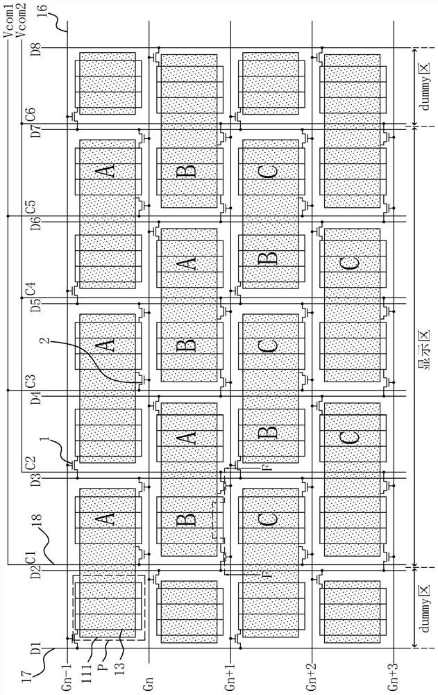
[0036] The array substrate 10 is provided with a plurality of scanning lines 16 and a plurality of data lines 17, and the plurality of scanning lines 16 and the plurality of data lines 17 are insulated from each other to define a plurality of pixel units P arranged in an array, and each pixel A pixel electrode 13 is disposed in the unit P, and each pixel electrode 13 is connected to a scan line 16 and a data line 17 adjacent to the first switch element 1 through the first switch element 1 .
[0037]A plurality of common lines 18 (marked by C1, C2, C3...) and a plurality of common electrode blocks 111 are also provided on the array substrate 1...
no. 2 example
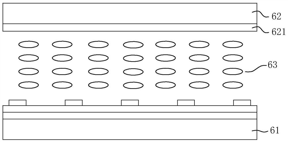
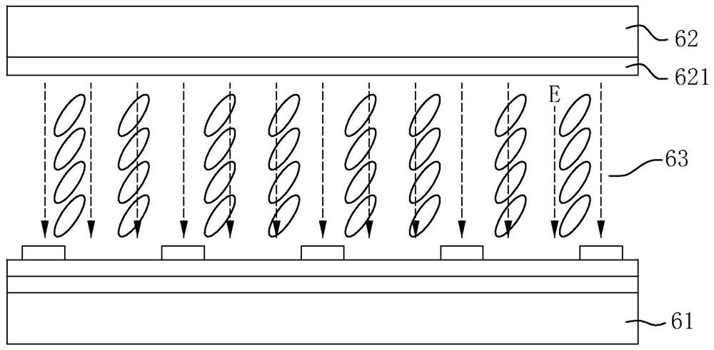
[0064] Please refer to Figure 8 and Figure 9 The difference between the liquid crystal display device provided by the second embodiment of the present invention and the first embodiment above is that the liquid crystal layer 30 in this embodiment uses negative liquid crystal molecules. With the advancement of technology, the performance of negative liquid crystal has been significantly improved, and its application has become more and more extensive. In this example, if Figure 8 As shown, in the initial state (that is, under the condition that no voltage is applied to the liquid crystal display device), the negative liquid crystal molecules in the liquid crystal layer 30 have a relatively large initial pretilt angle with respect to the substrate, that is, the negative liquid crystal molecules in the initial state are relative to the substrate. The substrate is in a tilted posture.
[0065] Narrow viewing angle mode: please refer to Figure 8 In this embodiment, in the n...
PUM
 Abstract
Description
Claims
Application Information
 - R&D Engineer
- R&D Manager
- IP Professional
- Industry Leading Data Capabilities
- Powerful AI technology
- Patent DNA Extraction
Browse by: Latest US Patents, China's latest patents, Technical Efficacy Thesaurus, Application Domain, Technology Topic, Popular Technical Reports.
© 2024 PatSnap. All rights reserved.Legal|Privacy policy|Modern Slavery Act Transparency Statement|Sitemap|About US| Contact US: help@patsnap.com