Display panel and display device

A technology for display panels and display devices, which can be applied to instruments, semiconductor devices, optics, etc., and can solve problems such as poor display effect of display panels.

Active Publication Date: 2021-09-21
SHANGHAI TIANMA MICRO ELECTRONICS CO LTD
View PDF7 Cites 0 Cited by
  • Summary
  • Abstract
  • Description
  • Claims
  • Application Information

AI Technical Summary

Problems solved by technology

[0003] In view of this, the present invention provides a display panel and a display device, which effectively solve the problem of poor display effect of existing display panels

Method used


Image

  • Display panel and display device
  • Display panel and display device
  • Display panel and display device

Examples


Embodiment Construction

[0034] The following will clearly and completely describe the technical solutions in the embodiments of the present invention with reference to the accompanying drawings in the embodiments of the present invention. Obviously, the described embodiments are only some, not all, embodiments of the present invention. Based on the embodiments of the present invention, all other embodiments obtained by persons of ordinary skill in the art without making creative efforts belong to the protection scope of the present invention.

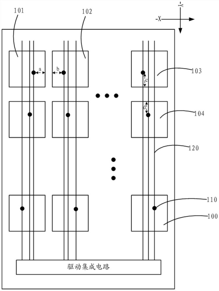
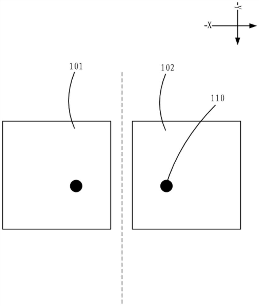
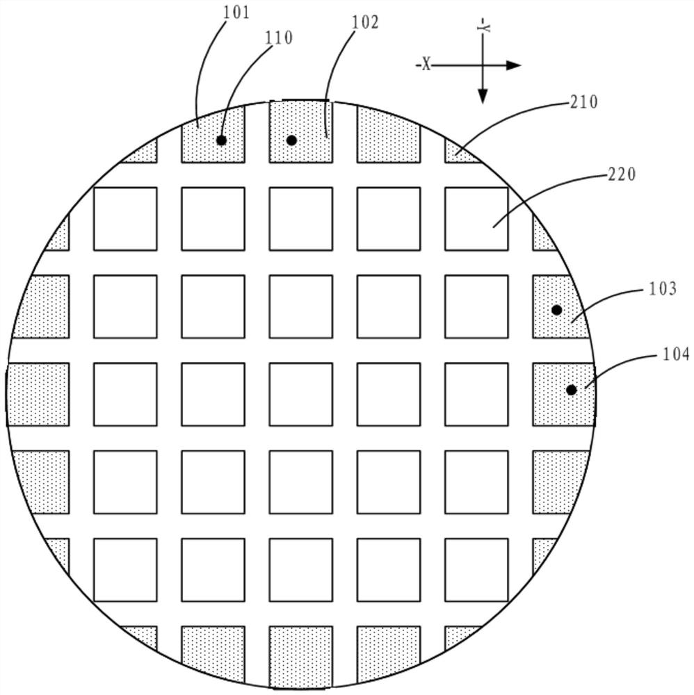
[0035] As mentioned in the background technology, the self-capacitance touch method can be: divide the transparent conductive layer used as the common (VCOM) electrode on the array substrate into several squares as touch electrodes, and then use specific electrode traces to The control electrode is connected, and one end of the electrode trace is connected to the driver integrated circuit. When the finger or the touch structure touches the self-capacitance touc...


PUM


Abstract

The invention discloses a display panel and a display device, which effectively solves the problem of a large difference in the delay of transmission signals between two adjacent areas on opposite sides of touch electrodes in the row direction and the column direction, and ensures the display effect of the display panel. high. In addition, by setting the main signal terminal of the third touch electrode and the main signal terminal of the fourth touch electrode in the column direction in a non-overlapping shape, so that the plurality of electrode leads connected to the corresponding main signal terminals are connected along the column. When the direction is extended, there will be no intersection of different electrode leads, and there is no need to set jumper wires connecting the electrode leads and the main signal end, reducing the number and difficulty of wiring.

Description

technical field [0001] The present invention relates to the field of display technology, and more specifically, to a display panel and a display device. Background technique [0002] At present, in order to realize the thinning and lightening of the touch panel, the research on the integration of the touch panel and the liquid crystal display panel is becoming more and more popular. Among them, an in-cell (In-Cell) touch solution in which a touch panel is embedded in a liquid crystal display panel has attracted widespread attention. In-Cell touch solutions include self-capacitance touch and mutual-capacitance touch. Among them, the self-capacitance touch method can be: divide the transparent conductive layer used as the common (VCOM) electrode on the array substrate into several squares as touch electrodes, and then use specific electrode traces to communicate with the touch electrodes through via holes. And one end of the electrode trace is connected to the driving integr...

Claims


Application Information

Patent Timeline
Patent Type & Authority Patents(China)
IPC IPC(8): G02F1/1333G02F1/1343H01L27/32
CPCG02F1/13338G02F1/134309H10K59/40
Inventor 楼腾刚
Owner SHANGHAI TIANMA MICRO ELECTRONICS CO LTD
Why Eureka
Try Eureka