
Patsnap Eureka
For R&D, Patsnap Eureka makes reading and utilizing patents & technical documents easy.
Patsnap Eureka AIR
Designed for self-driven R&D workflows. Generate viable solutions, solve complex R&D challenges, empower your innovation with AI.

Patsnap Eureka Materials
Designed for material experts only. Revolutionize your material R&D, from search, analyze, to developing new materials.

TechResearch
Generate reliable direction feasibility study reports for your R&D in just a few steps.

TechSeek
Discover and master advanced knowledge NOW. Basics, ideas, possibilities, all at once.

TechMind
As an expert in R&D Theories, TechMind can generates customized viable solutions instantly.

TechRisk
Analyze your overall solution with one click, know your potential R&D risks in advance.

TechMonitor
Get weekly tech updates, stay abreast of the latest tech innovations and key insights.
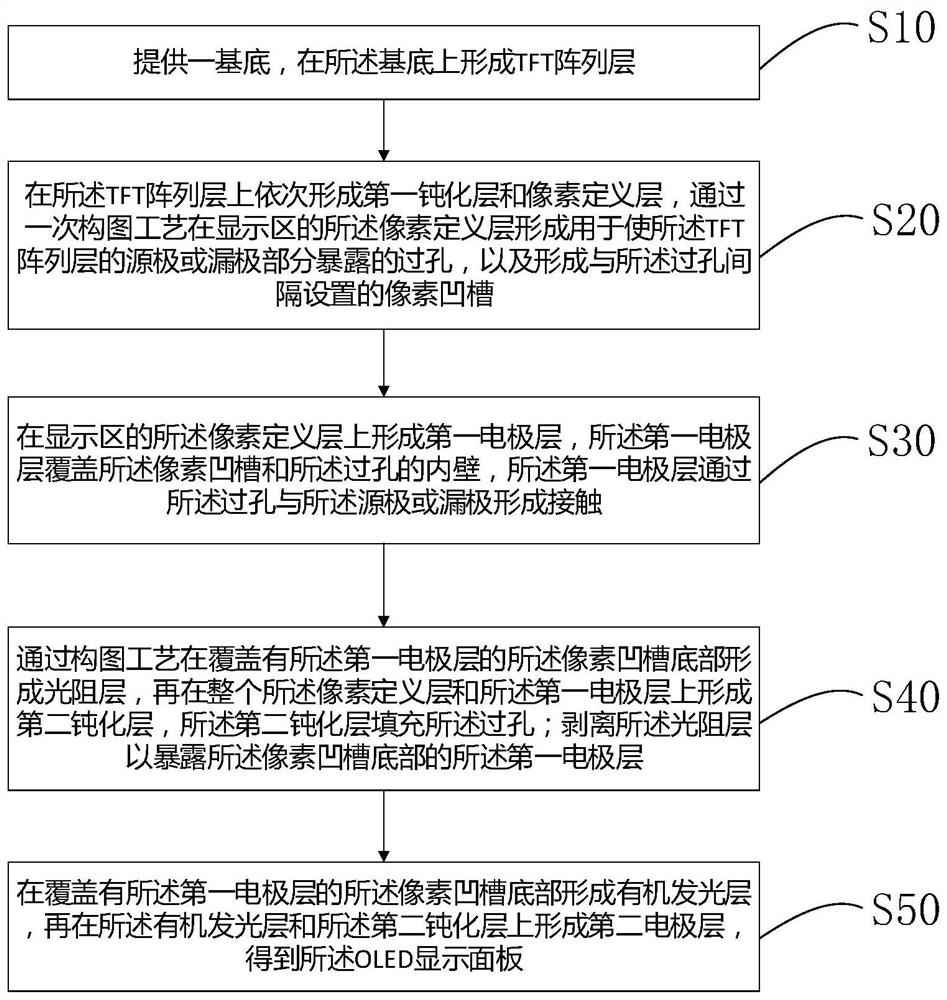
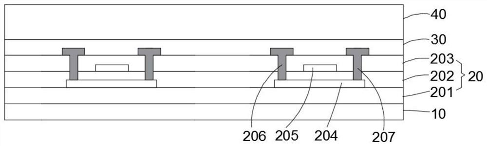
A kind of preparation method of oled display panel and oled display panel, display device
A display panel and display area technology, which is applied in semiconductor/solid-state device manufacturing, semiconductor devices, electrical components, etc., can solve problems such as light leakage, color saturation reduction, and improvement of display image quality, so as to reduce production costs and achieve long-term Long service life, good barrier effect against water vapor and oxygen
- Summary
- Abstract
- Description
- Claims
- Application Information
AI Technical Summary
Problems solved by technology
Method used
Image


Examples
Embodiment Construction
[0039] The following descriptions are preferred implementations of the embodiments of the present invention. It should be pointed out that those skilled in the art can make some improvements and modifications without departing from the principles of the embodiments of the present invention. These improvements And retouching are also regarded as the scope of protection of the embodiments of the present invention.
[0040] The terms "comprising" and "having" and any variations thereof appearing in the specification, claims and drawings of this application are intended to cover non-exclusive inclusion. For example, a process, method, system, product or device comprising a series of steps or units is not limited to the listed steps or units, but optionally also includes unlisted steps or units, or optionally further includes For other steps or units inherent in these processes, methods, products or apparatuses. In addition, the terms "first", "second", and "third", etc. are used ...
PUM
 Abstract
Description
Claims
Application Information
 - R&D Engineer
- R&D Manager
- IP Professional
- Industry Leading Data Capabilities
- Powerful AI technology
- Patent DNA Extraction
Browse by: Latest US Patents, China's latest patents, Technical Efficacy Thesaurus, Application Domain, Technology Topic, Popular Technical Reports.
© 2024 PatSnap. All rights reserved.Legal|Privacy policy|Modern Slavery Act Transparency Statement|Sitemap|About US| Contact US: help@patsnap.com