Memory structure

A memory and storage layer technology, applied in the semiconductor field, can solve problems such as leakage and affect memory performance, and achieve the effect of improving erasing efficiency

Pending Publication Date: 2018-12-18
YANGTZE MEMORY TECH CO LTD
View PDF10 Cites 18 Cited by
  • Summary
  • Abstract
  • Description
  • Claims
  • Application Information

AI Technical Summary

Problems solved by technology

However, the doped well is prone to problems such as leakage with the substrate and between adjacent doped wells, which affects the performance of the memory.

Method used


Image

  • Memory structure
  • Memory structure
  • Memory structure

Examples


Embodiment Construction

[0018] The specific implementation of the memory structure provided by the present invention will be described in detail below in conjunction with the accompanying drawings.

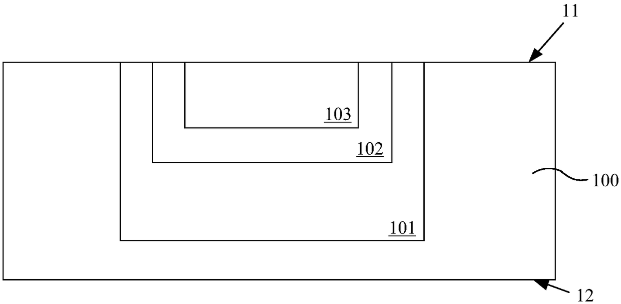
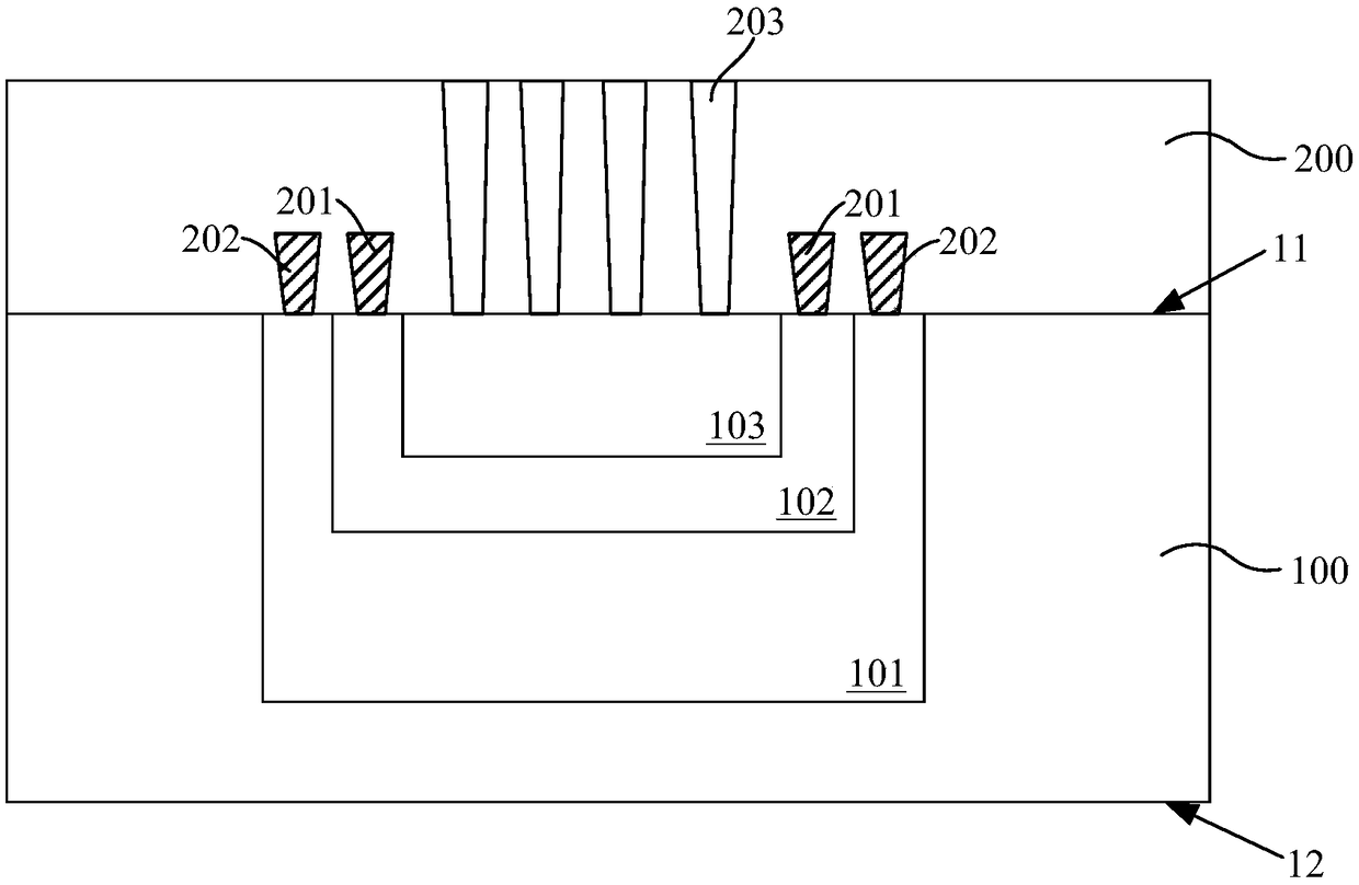
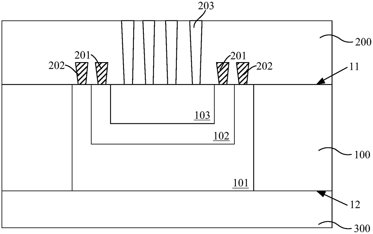
[0019] Please refer to Figure 1 to Figure 4 It is a structural schematic diagram of the formation process of the memory structure according to a specific embodiment of the present invention.

[0020] Please refer to figure 1 , providing a substrate layer 100, the substrate layer 100 has an opposite first surface 11 and a second surface 12; a conductive region is formed in the substrate layer 100, and the top of the conductive region faces the first surface of the substrate layer 100 surface 11 , the bottom of the conductive region faces the second surface 12 of the substrate layer 100 .

[0021] The substrate layer 100 is a semiconductor material layer, which may be a single crystal silicon wafer, a semiconductor epitaxial layer including a single crystal silicon wafer and the surface of the wafer, or...


PUM


Abstract

A memory structure includes a substrate layer having opposite first and second surfaces, a conductive region formed therein, a top portion of the conductive region facing a first surface of the substrate layer and a bottom portion of the conductive region facing a second surface of the substrate layer, and a bottom portion of the conductive region facing a second surface of the substrate layer. Astorage layer located on a first surface of the substrate layer; An isolation structure penetrating through the substrate layer and located at the edge of the conductive region, and arranged around the conductive region for isolating the conductive region from the substrate layer of the periphery of the isolation structure; The conductive region includes a shield layer located at the bottom of theconductive region and a P-type doped well located above the shield layer. The performance of the memory is improved.

Description

technical field [0001] The invention relates to the technical field of semiconductors, in particular to a memory structure. Background technique [0002] In recent years, the development of flash memory (Flash Memory) is particularly rapid. The main feature of flash memory is that it can keep stored information for a long time without power on, and has the advantages of high integration, fast access speed, easy erasing and rewriting, etc. Has been widely used. In order to further increase the bit density (Bit Density) of the flash memory while reducing the bit cost (Bit Cost), three-dimensional flash memory (3D NAND) technology has been developed rapidly. [0003] The storage array of 3D NAND is formed on the surface of the substrate, which is usually a P-type substrate, and doped wells are also formed in the substrate, including N-type doped wells and located in the N-type doped wells. P-type doped well. The doped well and the substrate form a PNP type doped structure. ...

Claims


Application Information

Patent Timeline
Patent Type & Authority Applications(China)
IPC IPC(8): H01L27/11551H01L27/11578H10B41/20H10B43/20
CPCH10B41/20H10B43/20
Inventor 夏志良陈俊鲍琨董金文华文宇靳磊江宁刘峻
Owner YANGTZE MEMORY TECH CO LTD
Why Eureka
Try Eureka