A charge-pump method for calculating stress-induced changes in interface state density in nano-cmos devices

A technology of interface state density and charge pump, which is applied in the direction of measuring electricity, measuring electrical variables, testing a single semiconductor device, etc., can solve problems that affect the accuracy of measurement results, and achieve the effect of promoting the development of research and high accuracy

Active Publication Date: 2020-12-22
马丽娟
View PDF7 Cites 0 Cited by
  • Summary
  • Abstract
  • Description
  • Claims
  • Application Information

AI Technical Summary

Problems solved by technology

However, during the implementation of this method, the leakage current changes with the measurement frequency, which ultimately affects the accuracy of the measurement results.

Method used


Image

  • A charge-pump method for calculating stress-induced changes in interface state density in nano-cmos devices
  • A charge-pump method for calculating stress-induced changes in interface state density in nano-cmos devices
  • A charge-pump method for calculating stress-induced changes in interface state density in nano-cmos devices

Examples


Embodiment 1

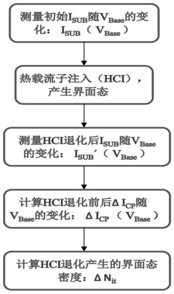
[0046] In the present embodiment, the CMOS device parameter used is that L (channel length) is 45nm, W (channel width)=10 μm, T OX (Oxide layer thickness) = 2.6nm, N A (Channel doping) = 1E20 / cm 3 . according to figure 1 As shown in the flow chart, the specific charge pump method for calculating the stress-induced interface state density change in the nanometer CMOS device in this embodiment is as follows:

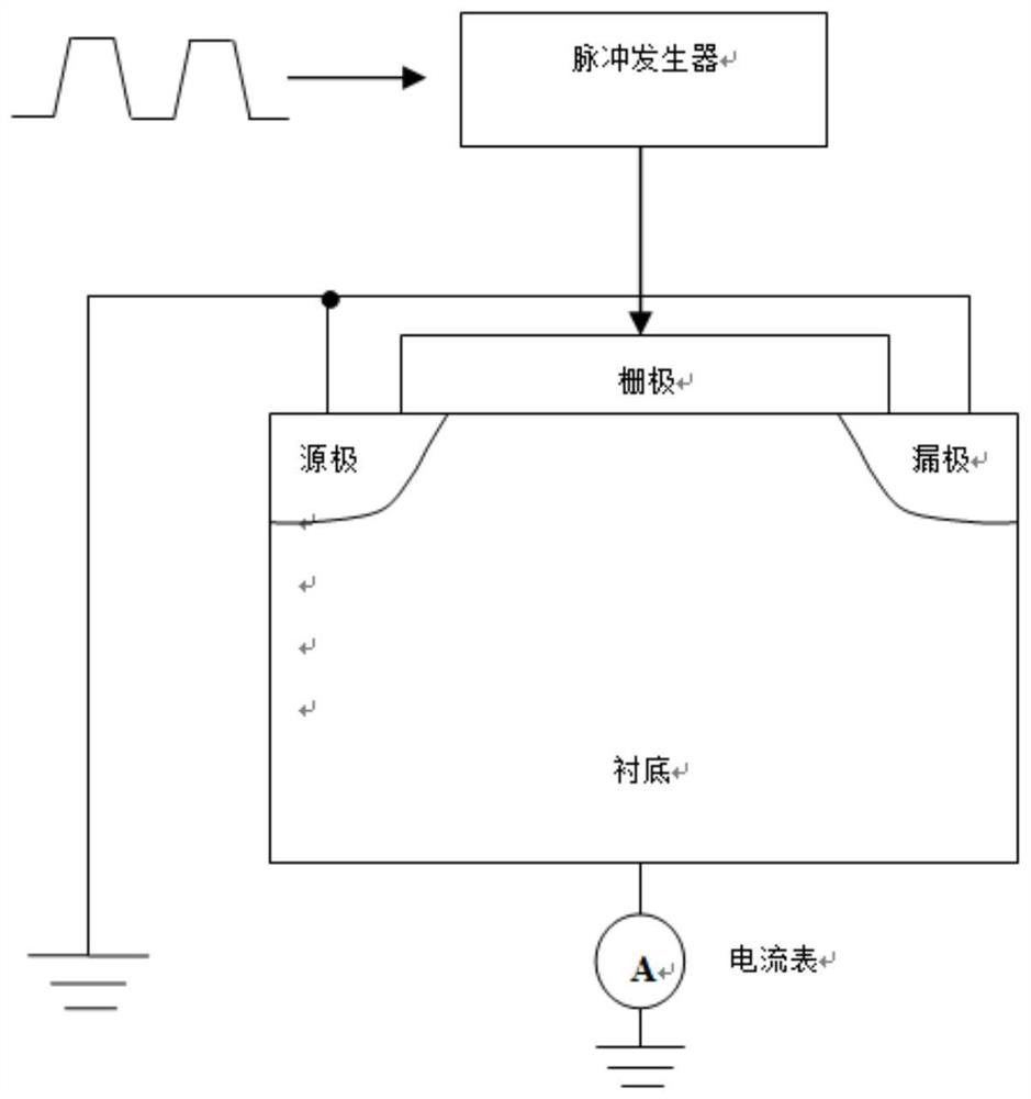
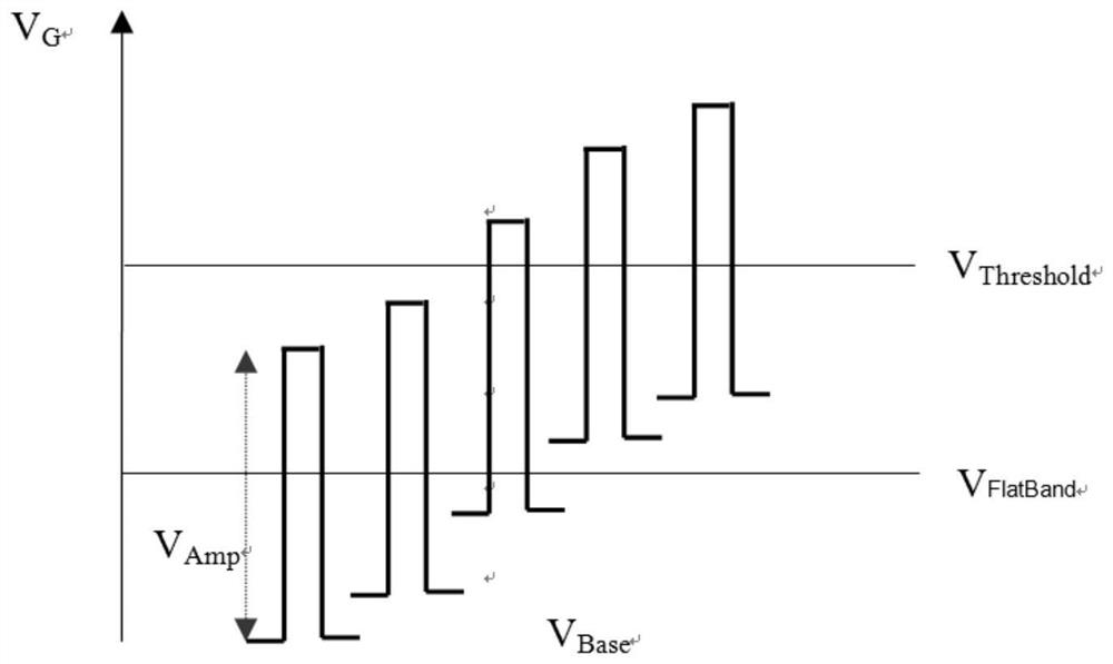
[0047] 1. In a CMOS device, measure the substrate current I SUB (I CP +I Leakage ) varies with substrate voltage V Base change curve. figure 2 The basic experimental setup of the charge pump test technology implemented in this implementation is given. For a CMOS device, the source, drain and substrate are grounded, and the substrate is connected to an ammeter at the same time to measure the current I from the gate to the substrate. SUB , the gate is connected to a voltage pulse generator. Apply voltage pulses to the grid for fixed-amplitude scanning, keep the pul...


PUM


Abstract

The invention discloses a charge pump method for calculating the variable quantity of stress-induced interfacial state density in a nano-CMOS device. On the basis of a traditional CP method, the substrate currents of the nano small-size device in an initial state and in a stress state are measured, the real charge pump current I<cp> is extracted from the substrate current, and the stress-induced interfacial defect density is calculated. The charge pump method is suitable for the nano small-size CMOS device with the large leakage current, the frequency is kept fixed in the measurement process,and measurement results are high in accuracy; and the research on a stress-induced defect characterization method of the nano-CMOS device can be further developed, and the development of reliability research of the nano small-size CMOS device is promoted advantageously.

Description

technical field [0001] The invention belongs to the technology of interface state density generated by stress of CMOS components, and in particular relates to a charge pump method for calculating stress-induced interface state density variation in nanometer CMOS devices. Background technique [0002] With the continuous development of integrated circuit technology, the technology node of integrated circuits is gradually reduced to the nanometer level, and the reliability of semiconductor devices seriously restricts the life of the devices. The stress conditions affecting CMOS devices mainly include: negative gate voltage temperature instability (Negative Bias Temperature Instability, NBTI), hot carrier injection effect (HotCarrier Injection, HCI) and gate oxide layer breakdown over time (Time-dependence dielectricbreakdown , TDDB) etc. When these stresses are applied in CMOS devices, the Si / SiO 2 The interface state or oxide layer defects are generated in the interface and...

Claims


Application Information

Patent Timeline
Patent Type & Authority Patents(China)
IPC IPC(8): G01R31/26
CPCG01R31/2601G01R31/2642
Inventor 马丽娟鲁明亮王旭吴建宁朱增力马先良
Owner 马丽娟
Why Eureka
Try Eureka