Dielectric-metal photonic crystal, preparation method thereof and tera-hertz pulse generator
A metal photonic crystal and dielectric technology, applied in the field of terahertz optoelectronic devices, can solve the problems of emission intensity limitation, limitation of production efficiency, etc., and achieve the effects of terahertz intensity enhancement, terahertz intensity enhancement, and polarization adjustment
- Summary
- Abstract
- Description
- Claims
- Application Information
AI Technical Summary
Problems solved by technology
Method used
Image
Examples
preparation example Construction
[0053] The present invention also provides a method for preparing the dielectric-metal photonic crystal described in the above technical solution, comprising the following steps:
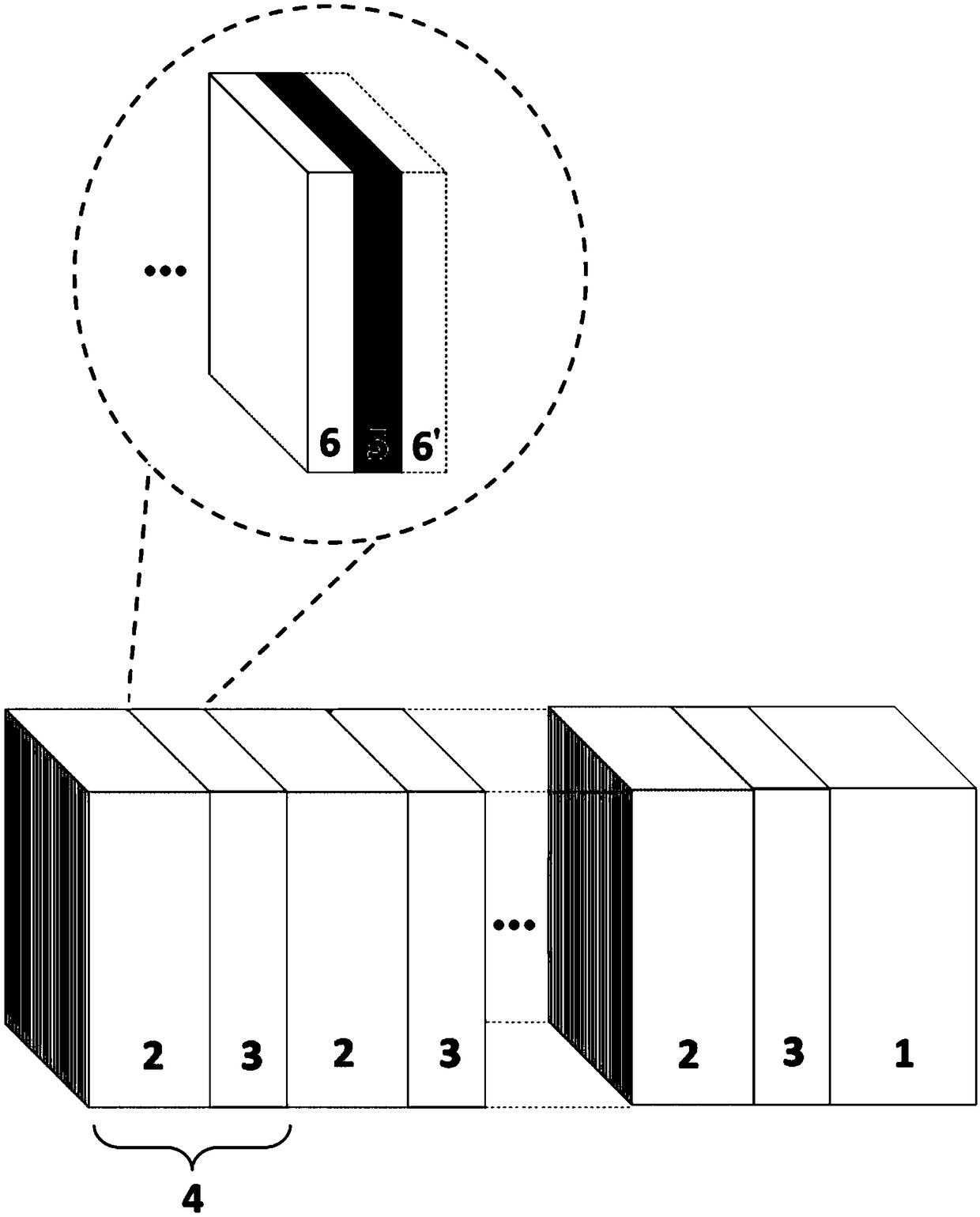
[0054] a) metal layer and dielectric layer are periodically deposited successively on the insulating substrate to obtain a dielectric-metal photonic crystal; the dielectric-metal photonic crystal has a multilayer composite structure shown in formula (I):
[0055] [Dielectric layer / Metal layer] n / insulating substrate formula (I);
[0056] In formula (I), n is an integer between 1~10;
[0057] The metal layer is a multi-layer structure formed by alternate compounding of magnetic nano-films and non-magnetic nano-films.
[0058] In the present invention, the insulating substrate, the metal layer and the dielectric layer are the same as those described in the above technical solution, and will not be repeated here.
[0059] In the present invention, the process of periodically and sequentially depos...
Embodiment 1
[0074] Put the MgO insulating substrate with a thickness of 0.5mm into the magnetron sputtering vacuum chamber to evacuate, and the vacuum degree reaches 10 -5 Start sputtering at Pa; first use DC magnetron sputtering to grow a 2nm thick Fe magnetic nanofilm on the MgO insulating substrate, and then use DC magnetron sputtering to grow a 2nm thick Pt nonmagnetic nanofilm on the Fe magnetic nanofilm , so as to form a metal layer; then use radio frequency magnetron sputtering to grow 90nm thick SiO on the Pt non-magnetic nano film 2 Dielectric layer, forming a [dielectric layer / metal layer] periodic unit; the above process of forming a [dielectric layer / metal layer] periodic unit is repeated 3 times to obtain a dielectric-metal photonic crystal;
[0075] The dielectric-metal photonic crystal has a multilayer composite structure shown in the following formula:
[0076] [SiO 2 Dielectric layer / Pt non-magnetic nano film / Fe magnetic nano film] 3 / MgO insulating substrate.
Embodiment 2
[0078] Put the MgO insulating substrate with a thickness of 0.5mm into the magnetron sputtering vacuum chamber to evacuate, and the vacuum degree reaches 10 -5 Start sputtering at Pa; first use DC magnetron sputtering to grow 2nm thick W non-magnetic nano-films on the MgO insulating substrate, and then use DC magnetron sputtering to grow 2nm-thick Fe magnetic nano-films on the W non-magnetic nano-films Then use DC magnetron sputtering to grow a 2nm thick Pt nonmagnetic nanofilm on the Fe magnetic nanofilm to form a metal layer; then use radio frequency magnetron sputtering to grow a 110nm thick SiO on the Pt nonmagnetic nanofilm 2 Dielectric layer, forming a [dielectric layer / metal layer] periodic unit; the above process of forming a [dielectric layer / metal layer] periodic unit is repeated 3 times to obtain a dielectric-metal photonic crystal;
[0079] The dielectric-metal photonic crystal has a multilayer composite structure shown in the following formula:
[0080] [SiO 2 D...
PUM
| Property | Measurement | Unit |
|---|---|---|
| Thickness | aaaaa | aaaaa |
| Thickness | aaaaa | aaaaa |
Abstract
Description
Claims
Application Information
 - Generate Ideas
- Intellectual Property
- Life Sciences
- Materials
- Tech Scout
- Unparalleled Data Quality
- Higher Quality Content
- 60% Fewer Hallucinations
Browse by: Latest US Patents, China's latest patents, Technical Efficacy Thesaurus, Application Domain, Technology Topic, Popular Technical Reports.
© 2025 PatSnap. All rights reserved.Legal|Privacy policy|Modern Slavery Act Transparency Statement|Sitemap|About US| Contact US: help@patsnap.com


