Method and device of 3D imaging of microstructure optical film
An imaging method and imaging device technology, applied in optics, optical components, decorative art, etc., can solve the problems of long molding cycle, reduced possibility of packaging application, expensive mold molding equipment, etc., to reduce production cost and complexity degree of effect
- Summary
- Abstract
- Description
- Claims
- Application Information
AI Technical Summary
Problems solved by technology
Method used
Image
Examples
Embodiment 1
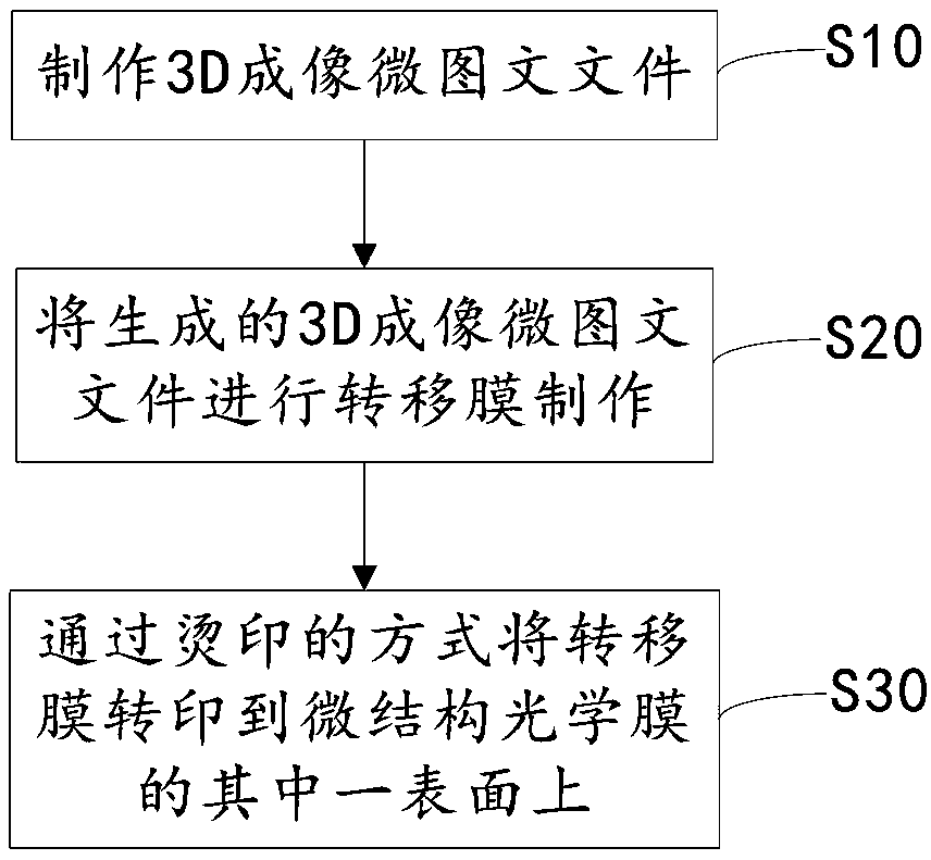
[0058] Such as Figure 1-9 Shown, the 3D imaging method of a kind of microstructure optical film of the present invention, this method comprises:
[0059] S10, making a 3D imaging micro-graphic file;
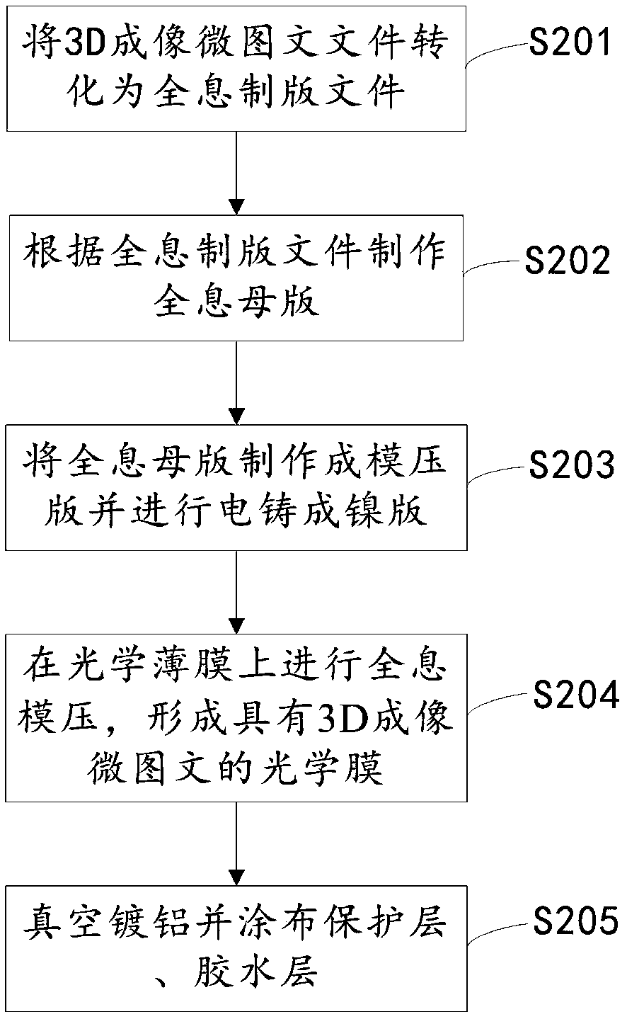
[0060] S20, making the transfer film of the generated 3D imaging micro-image file;
[0061] S30. Transfer the transfer film onto one of the surfaces of the microstructured optical film by means of hot stamping.
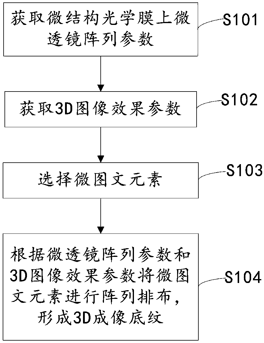
[0062] Specifically, a plurality of microlenses 21 are arrayed on the other surface of the microstructured optical film 2 . The design of 3D imaging micro-text is carried out through the relevant parameters of micro-lenses 21 arrayed on the other surface of the micro-structured optical film 2. The micro-text pattern can be text, logo, sign, number, etc., and the micro-text pattern Try to choose strokes and shapes that are relatively simple. Next, the 3D imaging micro-graphic file is made into a transfer film 1, and the transfer film transfer 1 is transferred to one ...
Embodiment 2
[0098] Such as Figure 10-11 As shown, the difference between this embodiment and the previous embodiment is that the way of hot stamping in this embodiment adopts the way of cold stamping, therefore, in this embodiment, the transfer film 1A includes a protective layer 15A, a micro-texture layer 14A, aluminum layer 13A, peeling layer 12A, and substrate layer 11A; protective layer 15A, microtexture layer 14A, aluminum layer 13A, peeling layer 12A, and substrate layer 11A are sequentially stacked from top to bottom. Under the action of UV cold transfer glue, the micro-texture layer 14A is transferred onto the second surface of the micro-structured optical film 2A, and the first surface of the micro-structured optical film 2A is arrayed with micro-lenses 21A.
[0099] In the cold transfer process, the adhesive layer 22A is uniformly coated on the designed position of the second surface of the microstructure optical film 2A by the cold transfer equipment, and then the cold transfe...
PUM
 Abstract
Description
Claims
Application Information
 - R&D Engineer
- R&D Manager
- IP Professional
- Industry Leading Data Capabilities
- Powerful AI technology
- Patent DNA Extraction
Browse by: Latest US Patents, China's latest patents, Technical Efficacy Thesaurus, Application Domain, Technology Topic, Popular Technical Reports.
© 2024 PatSnap. All rights reserved.Legal|Privacy policy|Modern Slavery Act Transparency Statement|Sitemap|About US| Contact US: help@patsnap.com


