Communication system based on FPGA and ASIC

A communication system and communication technology, applied in the field of optical communication, can solve the problems of lack of effective Li-Fi receiving modules, no power matching characteristics, low precision, etc., and achieve improved energy utilization, high power adaptation characteristics and versatility , The effect of low power consumption

Inactive Publication Date: 2018-11-23
苏州灵亿易电子科技有限公司
View PDF7 Cites 0 Cited by
  • Summary
  • Abstract
  • Description
  • Claims
  • Application Information

AI Technical Summary

Problems solved by technology

[0003] In view of the above-mentioned prior art, the purpose of the present invention is to provide a communication system based on FPGA and ASIC, which aims to solve the problem of high delay in the implementation of the clock signal used for Li-Fi encoding due to the existence of parasitic charges and residual charges in the prior art. , low precision, lack of effective Li-Fi receiving module and technical problems without power matching characteristics

Method used


Image

  • Communication system based on FPGA and ASIC
  • Communication system based on FPGA and ASIC
  • Communication system based on FPGA and ASIC

Examples


Embodiment 1

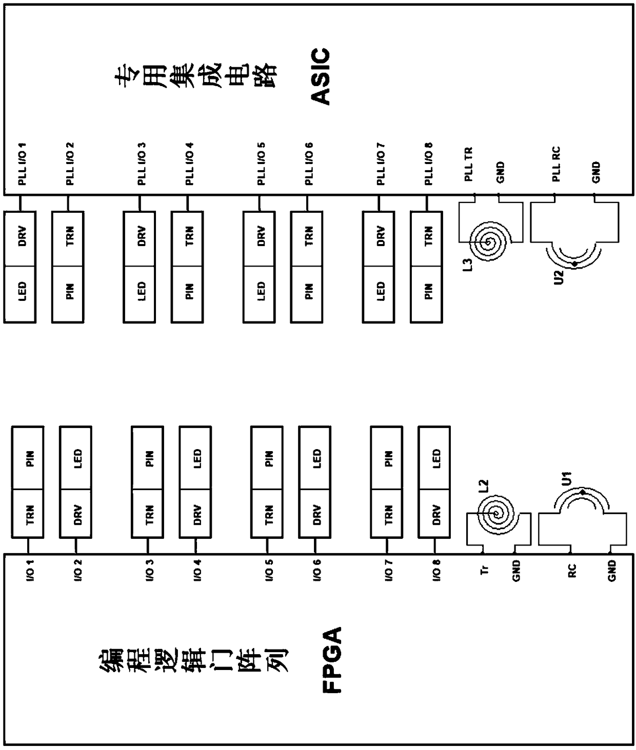
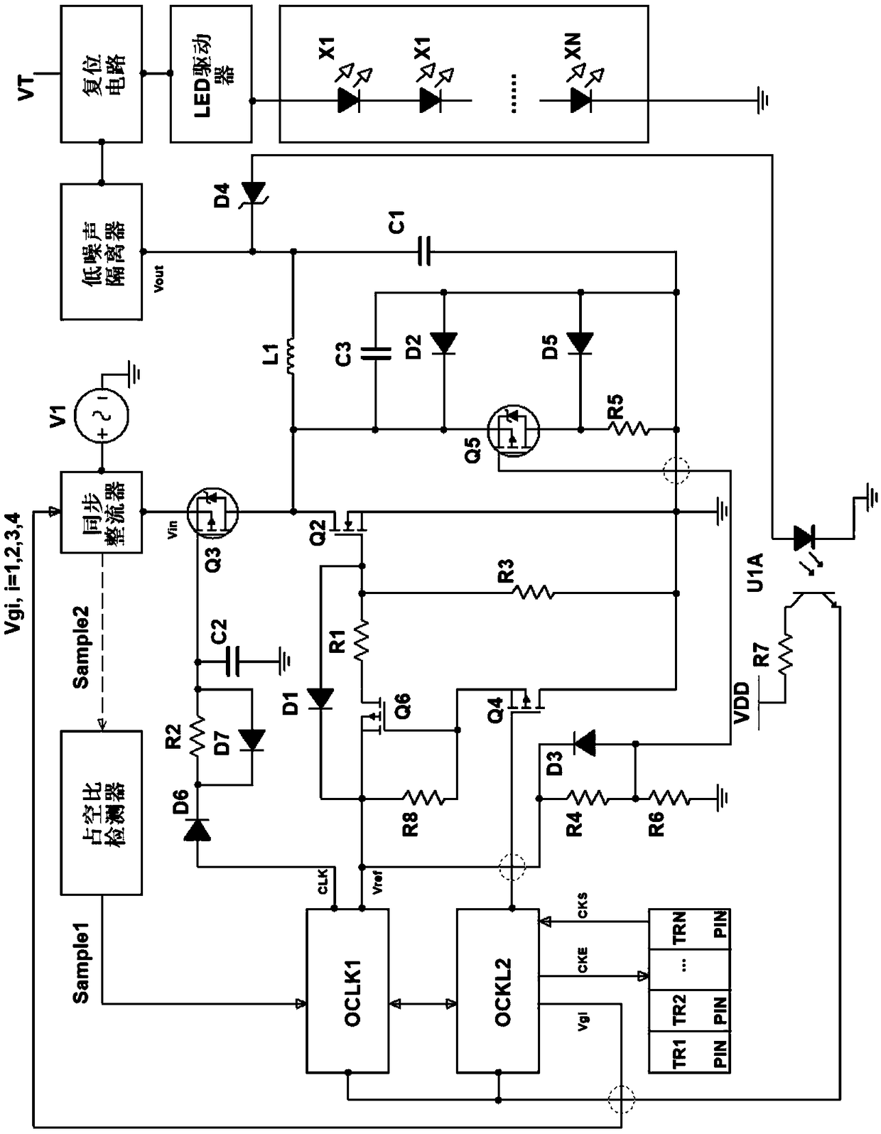
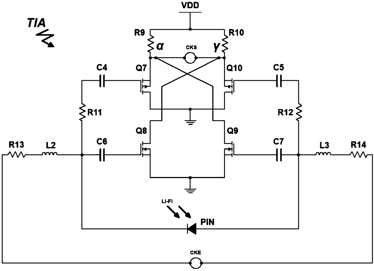
[0055] A communication system based on FPGA and ASIC, including:

[0056] Optical communication module, used for programming logic gate array and ASIC for Li-Fi signal communication;

[0057] Wireless fidelity communication module, used for programming logic gate array and ASIC for Wi-Fi signal compensation communication;

[0058] Wherein, the optical communication module receives the Li-Fi signal sent by the programming logic gate array through the delay-locked loop of the application-specific integrated circuit, or the optical communication module is driven by the delay-locked loop of the application-specific integrated circuit and sends the Li-Fi signal. signal to a programmable logic gate array, a delay-locked loop consists of a loop consisting of a low-pass filter, a phase detector, and a voltage-controlled oscillator.

[0059] In the above solution, the wireless fidelity communication module is correspondingly activated by the programming logic gate array or the applica...


PUM


Abstract

The invention discloses a communication system based on an FPGA and an ASIC, relating to the technical field of optical communication, and aiming to solve the technical problem that due to the presence of spurious charges and residual charges in the prior art, a clock signal for Li-Fi encoding has high delay and low precision during implementation, lacks an effective Li-Fi receiving module, and does not have power supply matching characteristics. The communication system mainly comprises an optical communication module and a wireless fidelity communication module, wherein the optical communication module is used for the field programmable gate array (FPGA) and the application-specific integrated circuit (ASIC) to perform Li-Fi signal communication; the wireless fidelity communication module is used for the FPGA and the ASIC to perform Wi-Fi signal compensation communication; and the optical communication module receives Li-Fi signals sent by the FPGA through a delay locked loop of theASIC, or the optical communication module is driven by the delay locked loop of the ASIC and transmits the Li-Fi signals to the FPGA. The scheme of the invention is used for the design of Li-FI communication circuits.

Description

technical field [0001] The invention relates to the technical field of optical communication, in particular to a communication system based on FPGA and ASIC. Background technique [0002] With the development of intelligent communication technology, power line carrier and wired interconnection have gradually evolved into radio interconnection. Nowadays, radio interconnection has also taken an important step towards the future, and Li-Fi optoelectronic interconnection has appeared. Li-Fi photoelectric interconnection currently mainly has difficulties in realizing the lossless transmission of signal clocks. Due to the parasitic charge of the switch and the accumulation of the residual charge of the capacitive and inductive devices in the power supply circuit and the drive circuit, when the power is turned on next time, the amplitude of the impact charge at the moment of turning on is very high, and it is easy to be damaged after being superimposed with the parasitic charge or...

Claims


Application Information

Patent Timeline
Patent Type & Authority Applications(China)
IPC IPC(8): H04B10/116H04B1/40
CPCH04B1/40H04B10/116
Inventor 卢征
Owner 苏州灵亿易电子科技有限公司
Why Eureka
Try Eureka