Dual-transistor silicon wafer cutter

A silicon wafer cutting, dual-transistor technology, used in work accessories, fine work devices, stone processing equipment, etc., can solve the problems of wafer collapse, lack of compression module compression, large blade wear, etc., to achieve uniform cutting , high cutting efficiency, the effect of improving the utilization rate

Inactive Publication Date: 2018-11-02
顾雨彤
View PDF1 Cites 1 Cited by
  • Summary
  • Abstract
  • Description
  • Claims
  • Application Information

AI Technical Summary

Problems solved by technology

However, the cutting of the blade of this equipment is a one-time cutting. On the one hand, it wears the blade greatly, and on the other hand, it is easy to break the silicon wafer during cutting. There is no pressing module to compress the silicon wafer during cutting to prevent the silicon wafer from moving.

Method used


Image

  • Dual-transistor silicon wafer cutter
  • Dual-transistor silicon wafer cutter
  • Dual-transistor silicon wafer cutter

Examples


Embodiment Construction

[0023] In order to make the technical means, creative features, goals and effects achieved by the present invention easy to understand, the present invention will be further described below in conjunction with specific embodiments.

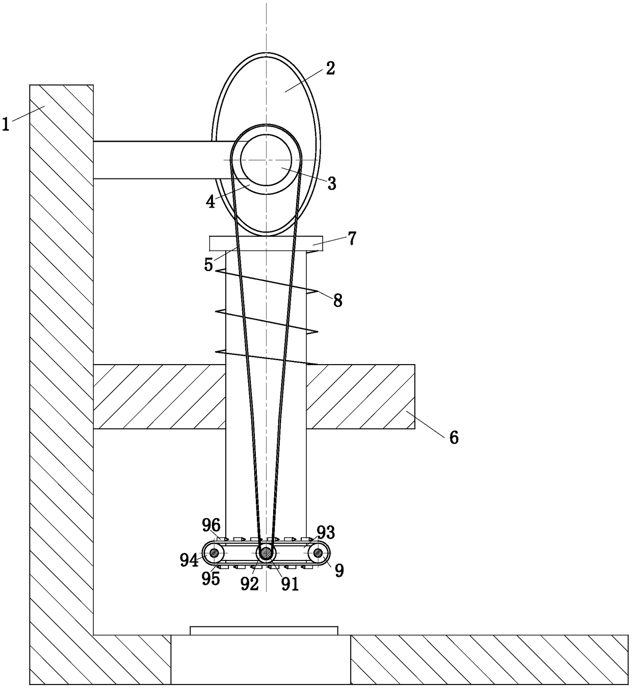
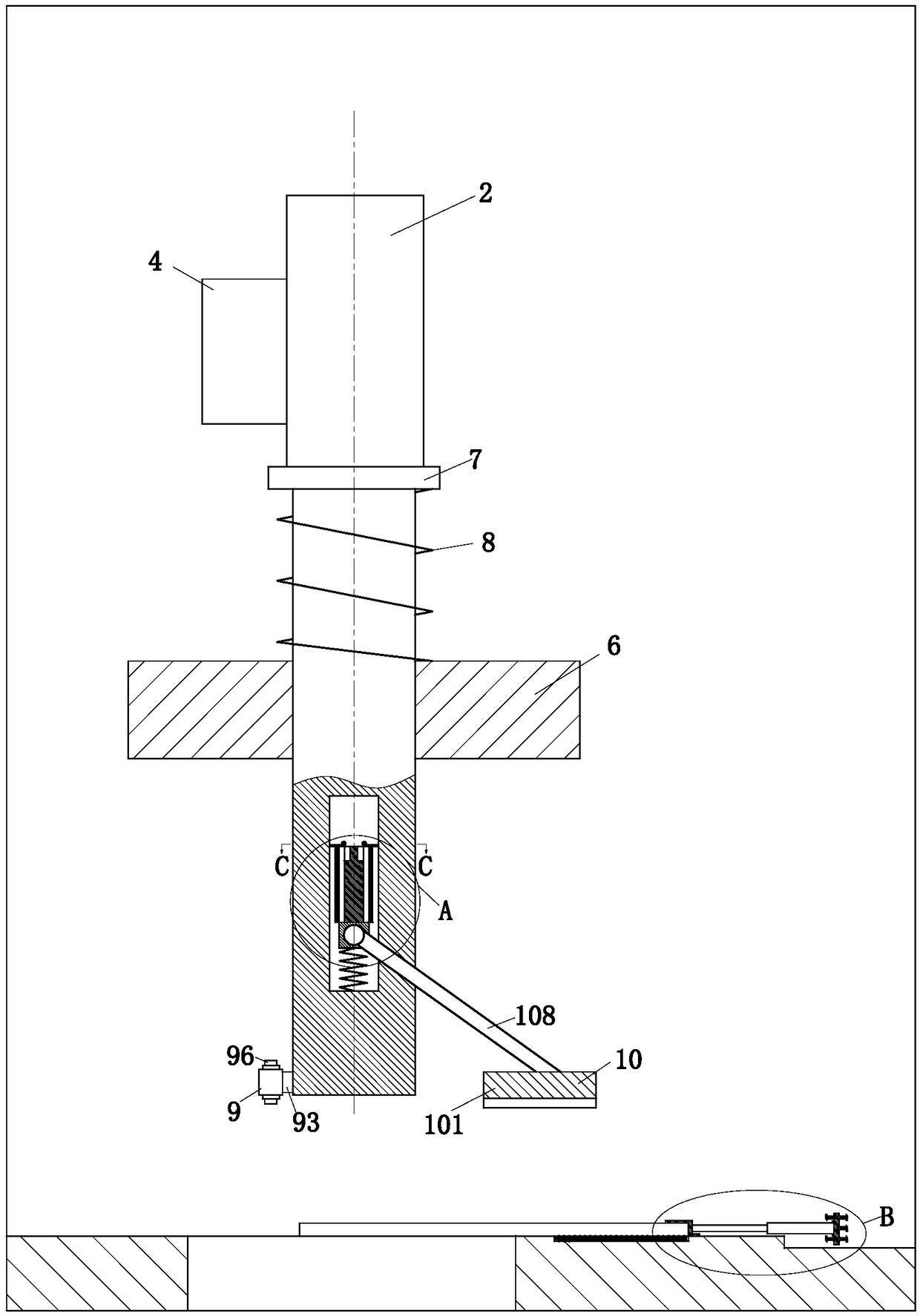
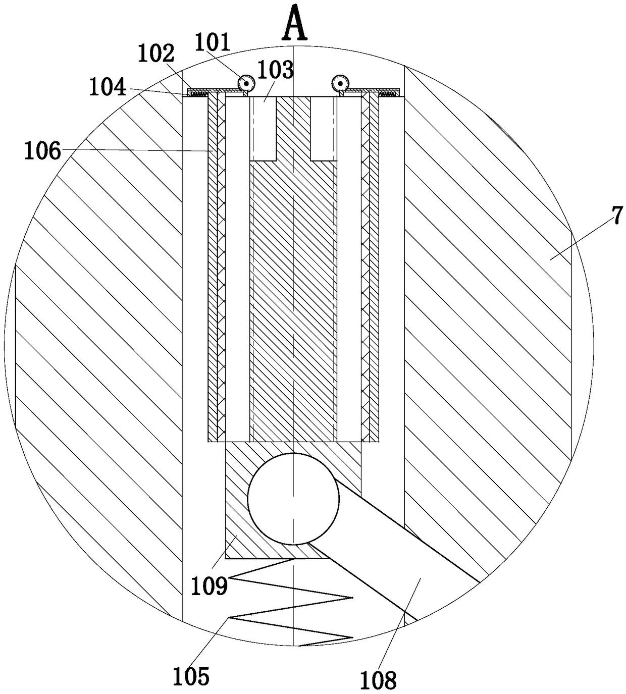
[0024] Such as Figure 1 to Figure 5 As shown, a kind of double-transistor silicon wafer cutter of the present invention comprises fixed mount 1, cam 2, motor one 3, pulley one 4, belt 5, guide bar 6, elevating bar 7 and spring one 8, also includes Cutting module 9, tablet pressing module 10 and pushing module 11, described motor one 3 is installed on the fixed frame 1 by pole; Described belt pulley one 4 is installed on the motor shaft of motor one 3; Described belt 5 Covered on the pulley-4; the cam 2 is installed on the motor shaft of the motor-3, and a circle of electromagnets is installed on the cam 2; the guide rod 6 is installed on the fixed frame 1, and the guide rod 6 is set There is a square hole; the lifting rod 7 passes through the sq...


PUM


Abstract

The invention belongs to the technical field of polysilicon wafer production, in particular to a dual-transistor silicon wafer cutter. The dual-transistor silicon wafer cutter comprises a fixing frame, a cam, a motor I, a belt pulley I, a belt, a guide rod, a lifting rod and a spring I; the dual-transistor silicon wafer cutter further comprises a cutting module, a wafer compacting module and a pushing module; the motor I is installed on the fixing frame through a strut; the belt pulley I is installed on a motor shaft of the motor I; the belt sleeves the belt pulley I; the cam is installed on the motor shaft of the motor I; the guide rod is installed on the fixing frame; the lifting rod is located at the lower part of the cam; one end of the spring I is fixed to the lifting rod; the cuttingmodule is used for cutting silicon wafers; the wafer compacting module is used for compacting the silicon wafers when the cutting module works; and the pushing module is used for pushing the siliconwafers to be right below the cutting module. The dual-transistor silicon wafer cutter is mainly used for carrying out quantitative cutting on the silicon wafers; the cutting is uniform; the assembly line production is achieved; the workload of workers is reduced; and the working efficiency is improved.

Description

technical field [0001] The invention belongs to the technical field of polycrystalline silicon wafer production, in particular to a double-transistor silicon wafer cutter. Background technique [0002] A transistor composed of two back-to-back PN structures to obtain voltage, current or signal gain. It originated from the point-contact transistor transistor invented in 1948, and developed into a junction transistor in the early 1950s, which is now called a bipolar transistor. There are two basic structures of bipolar transistors: PNP type and NPN type. In these three layers of semiconductors, the middle layer is called the base region, and the outer two layers are called the emitter region and the collector region. When a small amount of current is injected into the base region, a larger current will form between the emitter region and the collector region, which is the amplification effect of the transistor. [0003] There are also some technical solutions for silicon wa...

Claims


Application Information

Patent Timeline
Patent Type & Authority Applications(China)
IPC IPC(8): B28D5/04B28D7/04B28D7/00
CPCB28D5/04B28D5/0058B28D5/0082
Inventor 顾雨彤何显文
Owner 顾雨彤
Why Eureka
Try Eureka