Organic electroluminescent device
An electroluminescent device and a luminescent technology, which are applied in the direction of electric solid-state devices, electrical components, semiconductor devices, etc., can solve the problems of short luminous life, rapid device efficiency roll-off, etc., and achieve high luminous efficiency and lighten the phenomenon of efficiency roll-off , The effect of prolonging the luminous life
- Summary
- Abstract
- Description
- Claims
- Application Information
AI Technical Summary
Problems solved by technology
Method used
Image

Examples
Embodiment 1
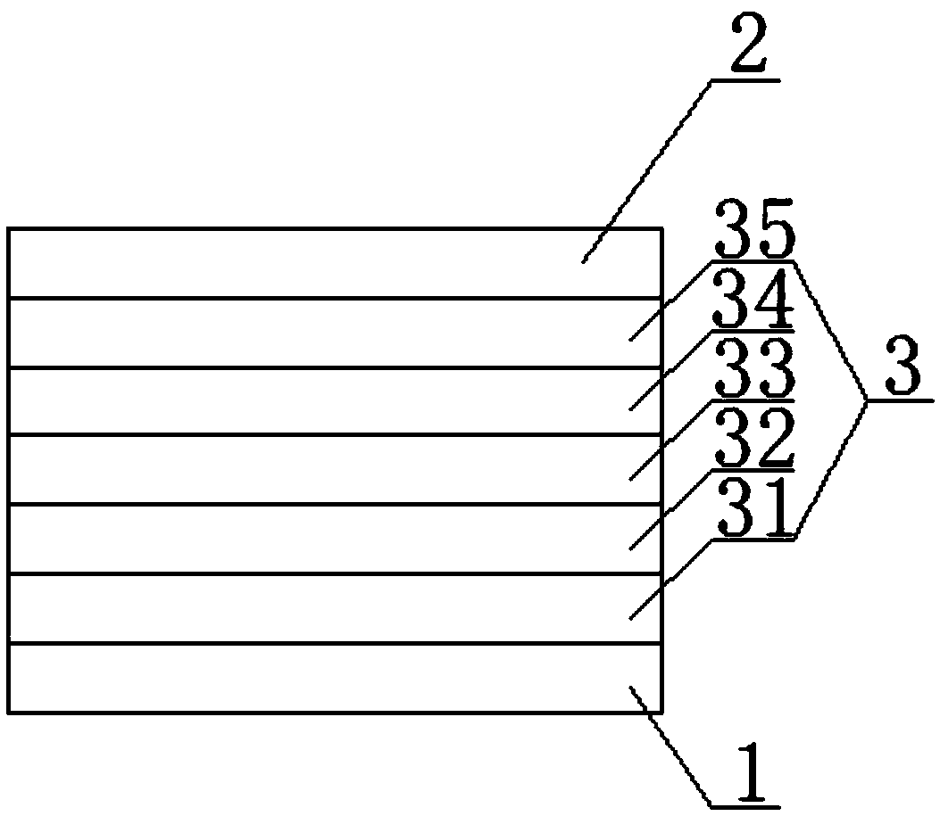
[0063] This embodiment provides an organic electroluminescent device, such as figure 2 As shown, it includes a first electrode 1, a second electrode 2 and an organic functional layer 3 between the first electrode 1 and the second electrode. Wherein, the first electrode 1 is an anode, the second electrode 2 is a cathode, and the organic functional layer 3 includes a hole injection layer 31, a hole transport layer 32, a light emitting layer 33, an electron transport layer 34 and Electron injection layer 35 .
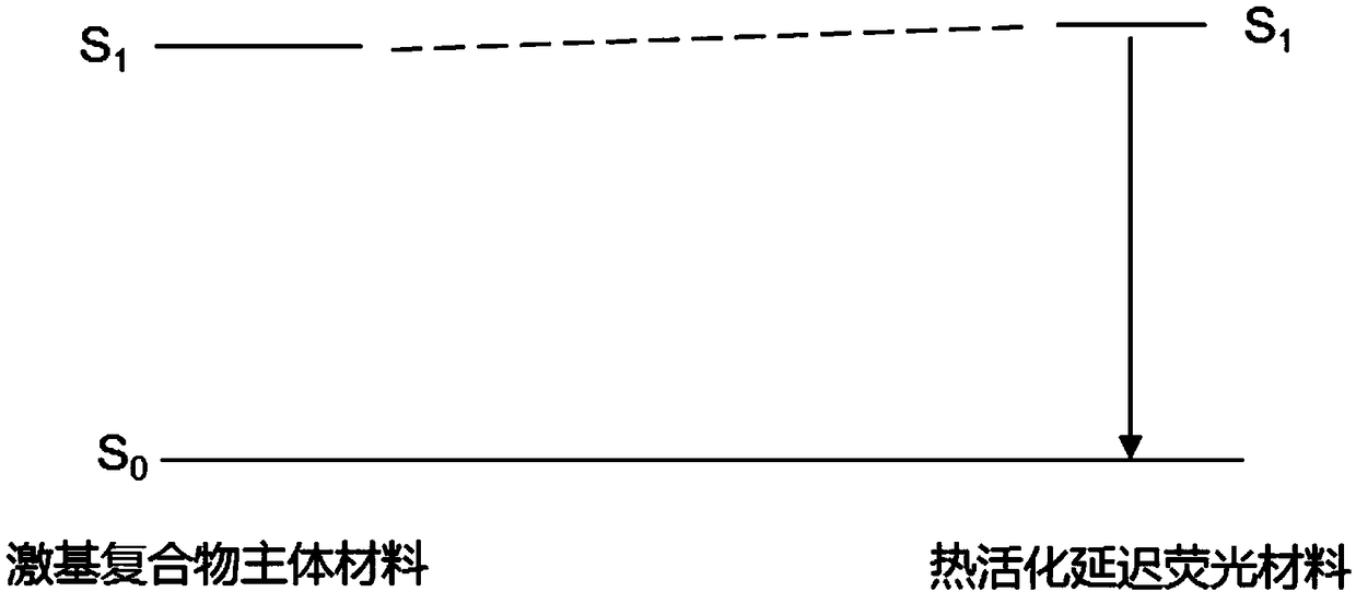
[0064] The light-emitting layer 33 is composed of a host material doped with a guest material, the host material is an exciplex with electron transport properties and hole transport properties, and the guest material is a thermally activated delayed fluorescent material, wherein the doping ratio of the thermally activated delayed fluorescent material is (The ratio of the mass of the thermally activated delayed fluorescent material to the total mass of the light-emitting ...
Embodiment 2
[0080] This embodiment provides an organic electroluminescent device. The structure of the organic electroluminescent device is the same as that in embodiment 1. The only difference between the organic electroluminescent device and the organic electroluminescent device provided in embodiment 1 is that an exciplex is formed. The mass ratio of electron donor material (D-20) and electron acceptor material (A-30) is 7:3. An organic electroluminescent device has the following device structure:
[0081] ITO / HATCN(5nm) / NPB(30nm) / TCTA(10nm) / 63wt% (D-20): 27wt% (A-30): 10wt% (T-3) (30nm) / 50wt% DpyPA: 50wt% Liq(30nm) / LiF(0.5nm) / Al(150nm).
[0082] The singlet energy level of the exciplex is 2.86eV, and the singlet energy level of the thermally activated delayed fluorescent material (T-3) is 2.90eV.
Embodiment 3
[0084]This embodiment provides an organic electroluminescent device. The structure of the organic electroluminescent device is the same as that in embodiment 1. The only difference between the organic electroluminescent device and the organic electroluminescent device provided in embodiment 1 is that the main body of the light-emitting layer 33 The material is an electron donor material (D-20) and an electron acceptor material (A-19) to form an exciplex, and the mass ratio of the electron donor material (D-20) to the electron acceptor material (A-19) is 1:1; the doping ratio of the thermally activated delayed fluorescent material (T-3) as the guest material in the light emitting layer 33 is 20wt%. An organic electroluminescent device has the following device structure:
[0085] ITO / HATCN(5nm) / NPB(30nm) / TCTA(10nm) / 40wt%(D-20):40wt%(A-19):20wt%(T-3)(30nm) / 50wt%DpyPA:50wt% Liq(,30nm) / LiF(0.5nm) / Al(150nm).
[0086] The singlet energy level of the exciplex is 2.86eV, and the sing...
PUM
 Abstract
Description
Claims
Application Information
 - R&D
- Intellectual Property
- Life Sciences
- Materials
- Tech Scout
- Unparalleled Data Quality
- Higher Quality Content
- 60% Fewer Hallucinations
Browse by: Latest US Patents, China's latest patents, Technical Efficacy Thesaurus, Application Domain, Technology Topic, Popular Technical Reports.
© 2025 PatSnap. All rights reserved.Legal|Privacy policy|Modern Slavery Act Transparency Statement|Sitemap|About US| Contact US: help@patsnap.com