Manufacturing method of printed circuit board and printed circuit board

A technology of printed circuit board and manufacturing method, which is applied in the direction of multi-layer circuit manufacturing and printed circuit components, etc., can solve the problems of difficult to guarantee the thickness uniformity of the dielectric layer, difficult to control the expansion and shrinkage of the sub-outer layer, and abnormal alignment. , to achieve the effect of ensuring the alignment between layers of the overall structure, improving the problem of large differences in expansion and contraction, and avoiding the occurrence of abnormalities

Inactive Publication Date: 2018-10-09
PEKING UNIV FOUNDER GRP CO LTD +1
View PDF3 Cites 4 Cited by
  • Summary
  • Abstract
  • Description
  • Claims
  • Application Information

AI Technical Summary

Problems solved by technology

In PCB design, due to the requirements of signal integrity, the requirements for the uniformity of the thickness of the corresponding dielectric layer are very high. Take a 10-layer PCB board as an example, such as Figure 1a Due to the principle of lamination, it is difficult to ensure the uniformity of the thickness of the corresponding dielectric layer in the conventional PCB structure shown, so the customer designs a special PCB structure such as Figure 1b As shown, this type of design is very difficult in PCB production, and the expansion and contraction of the sub-outer layer are difficult to control, and the requirements for inter-layer alignment cannot be guaranteed.
The main reason is that if Figure 1c In the conventional lamination method, due to the large difference in thermal expansion coefficient between the cover plate, tray and steel plate, the heating capacity of the cover plate, tray and steel plate is inconsistent when they are pressed together, and the temperature of the cover plate or tray will be transmitted to the PCB during heating. The expansion and contraction of the PCB L1 layer close to the cover or tray will have irregular deviations. Since the outermost layer of this special structure is the core structure, when the expansion and contraction caused by the external temperature are inconsistent, such as Figure 1b The L1 and L10 layers will change accordingly, but since L1, L2, L9, and L10 are core board structures, when L1, L10 expands and shrinks, L2, L9 layers will also change accordingly, so that the overall structure will be Abnormal alignment between L2 and L9 layers and other layers occurs

Method used


Image

  • Manufacturing method of printed circuit board and printed circuit board
  • Manufacturing method of printed circuit board and printed circuit board
  • Manufacturing method of printed circuit board and printed circuit board

Examples


Embodiment Construction

[0031] In order to understand the above objects, features and advantages of the present invention more clearly, the present invention will be further described in detail below with reference to the accompanying drawings and specific embodiments. It should be noted that the embodiments of the present application and the features in the embodiments may be combined with each other in the case of no conflict.

[0032] Many specific details are set forth in the following description to facilitate a full understanding of the present invention. However, the present invention can also be implemented in other ways different from those described herein. Therefore, the protection scope of the present invention is not limited to the specific details disclosed below. Example limitations.

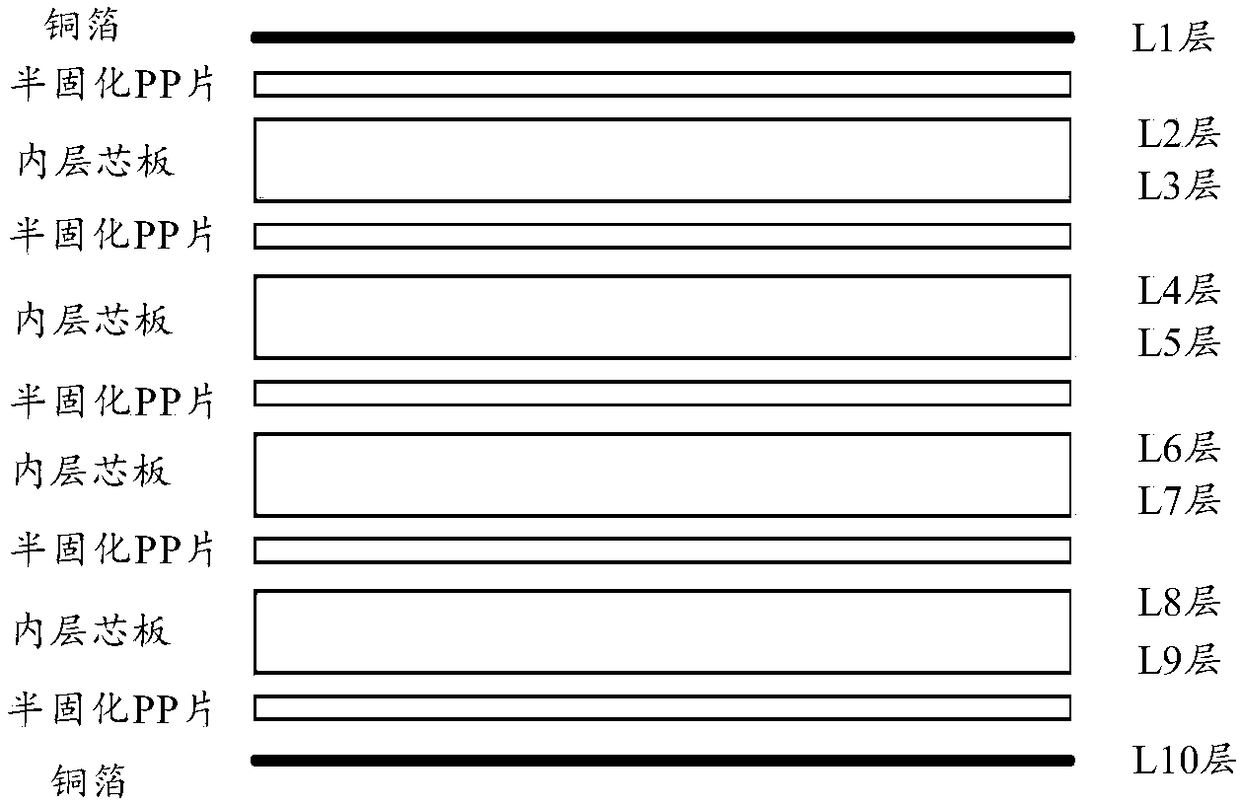
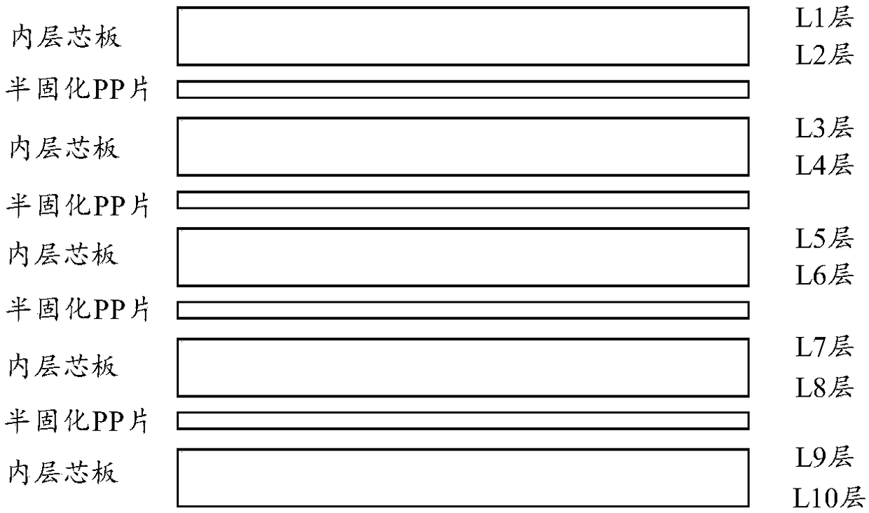
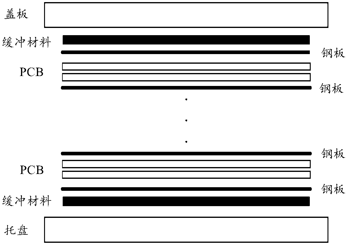
[0033] In an embodiment of the first aspect of the present invention, a method for manufacturing a printed circuit board is proposed, figure 2 A schematic flow chart of a method for manufacturing a pri...


PUM


Abstract

The invention provides a manufacturing method of a printed circuit board and a printed circuit board. The manufacturing method of the printed circuit board comprises the steps of manufacturing an inner layer for a core board of the printed circuit board; superimposing the core board to form a structure to be laminated; laminating the structure to be laminated by using a pseudo plate; manufacturingan outer layer for the laminated structure so as to form a printed circuit board. The manufacturing method can improve a problem of great expansion and shrinkage difference caused by the mismatchingbetween the thermal expansion coefficient of a steel plate and the thermal expansion coefficient of a material, enables the interlayer alignment of the whole structure to be guaranteed and avoids abnormal alignment.

Description

technical field [0001] The invention relates to the technical field of printed circuit boards, in particular to a method for manufacturing a printed circuit board and the printed circuit board. Background technique [0002] With the development of miniaturization, digitalization and high integration of electronic products, its signal transmission is also becoming increasingly high-frequency and high-speed, and higher performance and quality of PCB (Printed Circuit Board: printed circuit board) are also proposed. requirements, especially for high-speed circuit boards represented by communication products. Because it has high requirements on transmission rate and signal integrity, it not only has high requirements on the selection of production materials, but also puts forward strict requirements on its processing. In PCB design, due to the requirements of signal integrity, the requirements for the uniformity of the thickness of the corresponding dielectric layer are very hig...

Claims


Application Information

Patent Timeline
IPC IPC(8): H05K3/46H05K1/02
Inventor 柳小华徐榕李晓
Owner PEKING UNIV FOUNDER GRP CO LTD
Why Eureka
Try Eureka