Camera module and assembling method thereof
A camera module and lens assembly technology, which is applied in image communication, television, material gluing, etc., can solve the problems that the camera module cannot form clear image points and the image quality declines, so as to ensure the process yield, low cost, Effects that improve image quality
- Summary
- Abstract
- Description
- Claims
- Application Information
AI Technical Summary
Problems solved by technology
Method used
Image


Examples
no. 1 example
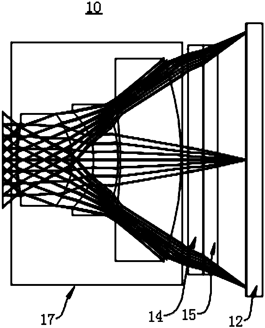
[0038] see figure 1 , this embodiment provides a camera module 10 , the camera module 10 includes an image sensor chip 12 , a filter 14 , a lens assembly 17 and a light-transmitting sheet 15 . The optical filter 14 is arranged between the image sensor chip 12 and the lens assembly 17 , and the light-transmitting sheet 15 is arranged between the image sensor chip 12 and the lens assembly 17 .
[0039] During the imaging process of the camera module 10, the optical path around the light is greater than the optical path in the center, and a light-transmitting sheet 15 is arranged between the image sensor chip 12 and the filter 14, and the light-transmitting sheet 15 can make the light focus on the periphery. Relative to the central focal point, the light is imaged on the curved imaging surface, which compensates for the defect of the curvature of the imaging surface caused by the warping of the image sensor chip 12 .
[0040] In this embodiment, the light-transmitting sheet 15 o...
no. 2 example
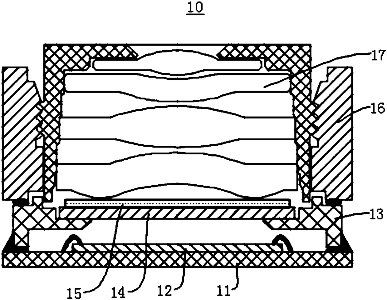
[0047] see image 3 , this embodiment provides a camera module 10, the camera module 10 is a fixed-focus module. The camera module 10 includes a PCB board 11 , an image sensor chip 12 , a filter holder 13 , a filter 14 , a light-transmitting sheet 15 , a lens holder 16 and a lens assembly 17 . The lens assembly 17 , the transparent sheet 15 , the optical filter 14 and the image sensor chip 12 are arranged in sequence.
[0048] The PCB board 11 is arranged on the side of the image sensor chip 12 away from the filter 14 , the image sensor chip 12 is bonded on the surface of the PCB board 11 , and the image sensor chip 12 and the PCB board 11 are electrically connected by gold wires.
[0049] PCB board 11, also known as printed circuit board, has an upper surface and an opposite lower surface, and is a provider of electrical connections for electronic components. Rigid PCB boards, flexible PCB boards, and rigid-flex boards can be used. Combine board. The image sensor chip 12 m...
no. 3 example
[0057] see Figure 4 , this embodiment provides a camera module 10, the camera module 10 is an auto-focus module. The camera module 10 includes a PCB board 11 , an image sensor chip 12 , a filter holder 13 , a filter 14 , a light-transmitting film 15 , a motor 18 and a lens assembly 17 . The lens assembly 17 , the transparent sheet 15 , the optical filter 14 and the image sensor chip 12 are arranged in sequence.
[0058] The PCB board 11 is arranged on the side of the image sensor chip 12 away from the filter 14 , the image sensor chip 12 is bonded on the surface of the PCB board 11 , and the image sensor chip 12 and the PCB board 11 are connected by gold wires.
[0059] The filter holder 13 is arranged between the PCB board 11 and the lens assembly 17, and the PCB board 11 and the filter holder 13 are bonded. The optical filter 14 is installed on the optical filter holder 13 , so that the optical filter 14 is arranged parallel to the image sensor chip 12 at intervals.
[0...
PUM
 Abstract
Description
Claims
Application Information
 - R&D
- Intellectual Property
- Life Sciences
- Materials
- Tech Scout
- Unparalleled Data Quality
- Higher Quality Content
- 60% Fewer Hallucinations
Browse by: Latest US Patents, China's latest patents, Technical Efficacy Thesaurus, Application Domain, Technology Topic, Popular Technical Reports.
© 2025 PatSnap. All rights reserved.Legal|Privacy policy|Modern Slavery Act Transparency Statement|Sitemap|About US| Contact US: help@patsnap.com