Semiconductor-apparatus packaging device

A device packaging and semiconductor technology, applied in the fields of semiconductor/solid-state device manufacturing, electrical components, circuits, etc., can solve the problems of inability to realize automatic turnover of semiconductor devices and troublesome operation.

Pending Publication Date: 2018-09-21
重庆市嘉凌新科技有限公司
View PDF0 Cites 3 Cited by
  • Summary
  • Abstract
  • Description
  • Claims
  • Application Information

AI Technical Summary

Problems solved by technology

Since the two sides of the semiconductor device need to be marked, after the semiconductor device is marked on one side, it is necessary to manually turn over the semiconductor device so that the other side of the semiconductor device is opposite to the marking head of the marking machine, so it is currently impossible To realize the automatic flipping of semiconductor devices, etc., the operation is more troublesome

Method used


Image

  • Semiconductor-apparatus packaging device
  • Semiconductor-apparatus packaging device
  • Semiconductor-apparatus packaging device

Examples


Embodiment Construction

[0017] The following is further described in detail through specific implementation methods:

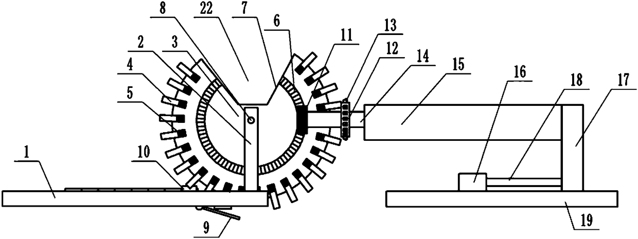
[0018] The reference signs in the drawings of the description include: the second processing table 1, the second support 2, the fan-shaped disc 3, the clamp 4, the pressing part 5, the rack 6, the notch surface 7, the guide rod 8, the discharge plate 9, the guide plate 10. Gear 11, marking disc 12, marking head 13, rotating shaft 14, marking machine 15, control button 16, first bracket 17, connecting rod 18, first processing table 19, pressing block 20, compression spring 21, Notch 22.

[0019] The embodiment is basically as attached Figure 1-Figure 4 Shown: a semiconductor device packaging device, including a first processing table 19 and a second processing table 1 located on the left side of the first processing table 19 . The first processing table 19 is rotatably connected with a first support 17 by a pin shaft, and a marking machine 15 is mounted on the first support 17 by a...


PUM


Abstract

The invention relates to a semiconductor-apparatus packaging device. The semiconductor-apparatus packaging device comprises a marking machine and a processing platform, wherein a first support is rotationally connected on the processing platform, a second support is fixed on the processing platform, and the marking machine is installed on the first support; a gear is rotationally connected on themarking machine, a plurality of marking heads are coaxially installed between the gear and the marking machine, and are evenly distributed with a circle of the gear as the center, and extruding switches abutting against a semiconductor apparatus are arranged on the marking heads; a sector disk is rotationally connected on the second support, a rack engaged with the gear is arranged on the sector disk, and comprises two connecting parts and two arc parts, angles of the arc parts are equal to the angle of the sector disk, lengths of the connecting parts are equal to the length of the sector disk, the arc parts are located on the two side faces of the sector disk respectively, the connecting parts are connected between the ends of the two arc parts, and a plurality of clamps are arranged on the sector disk, and are evenly distributed with the circle center of the sector disk as the center. According to the technical scheme, it is achieved that the two side faces of the semiconductor apparatus are automatically marked.

Description

technical field [0001] The invention relates to the field of semiconductor device processing, in particular to a semiconductor device packaging device. Background technique [0002] A semiconductor refers to a material whose conductivity at room temperature is between that of a conductor and an insulator. Semiconductors are widely used in radios, televisions, and temperature measurement. For example, diodes are devices made of semiconductors. A semiconductor is a material whose conductivity can be controlled, ranging from an insulator to a conductor. No matter from the perspective of technology or economic development, the importance of semiconductors is huge. The core units of most of today's electronic products, such as computers, mobile phones or digital recorders, are closely related to semiconductors. Common semiconductor materials include silicon, germanium, gallium arsenide, etc., and silicon is the most influential one in commercial applications among various semi...

Claims


Application Information

Patent Timeline
IPC IPC(8): H01L21/67H01L21/687
CPCH01L21/67282H01L21/68764
Inventor 罗妍
Owner 重庆市嘉凌新科技有限公司
Why Eureka
Try Eureka