
OLED display panel and display

A display panel and substrate technology, applied in the direction of electric solid-state devices, semiconductor devices, electrical components, etc., can solve the problems of narrow pixel gap, unfavorable printing technology production, low display brightness, etc., and achieve the effect of reducing resolution

Active Publication Date: 2018-09-07
BOE TECH GRP CO LTD +1
View PDF4 Cites 5 Cited by
  • Summary
  • Abstract
  • Description
  • Claims
  • Application Information

AI Technical Summary

Problems solved by technology

However, due to the increasingly higher resolution requirements in the TV market, the aperture ratio of OLED (Organic Light-Emitting Diode, Organic Light-Emitting Diode) devices is considerably compressed, resulting in problems such as shorter device life and lower display brightness.
In addition, the pixel gap of high-resolution products is narrow, which is not conducive to the use of printing technology, and the problem of color mixing often occurs due to the mixing of luminescent materials.

Method used


Image

  • OLED display panel and display
  • OLED display panel and display
  • OLED display panel and display

Examples


Embodiment Construction

[0011] The application will be further described in detail below in conjunction with the accompanying drawings and embodiments. It should be understood that the specific embodiments described here are only used to explain related inventions, rather than to limit the invention. It should also be noted that, for ease of description, only parts related to the invention are shown in the drawings.

[0012] It should be noted that, in the case of no conflict, the embodiments in the present application and the features in the embodiments can be combined with each other. The present application will be described in detail below with reference to the accompanying drawings and embodiments.

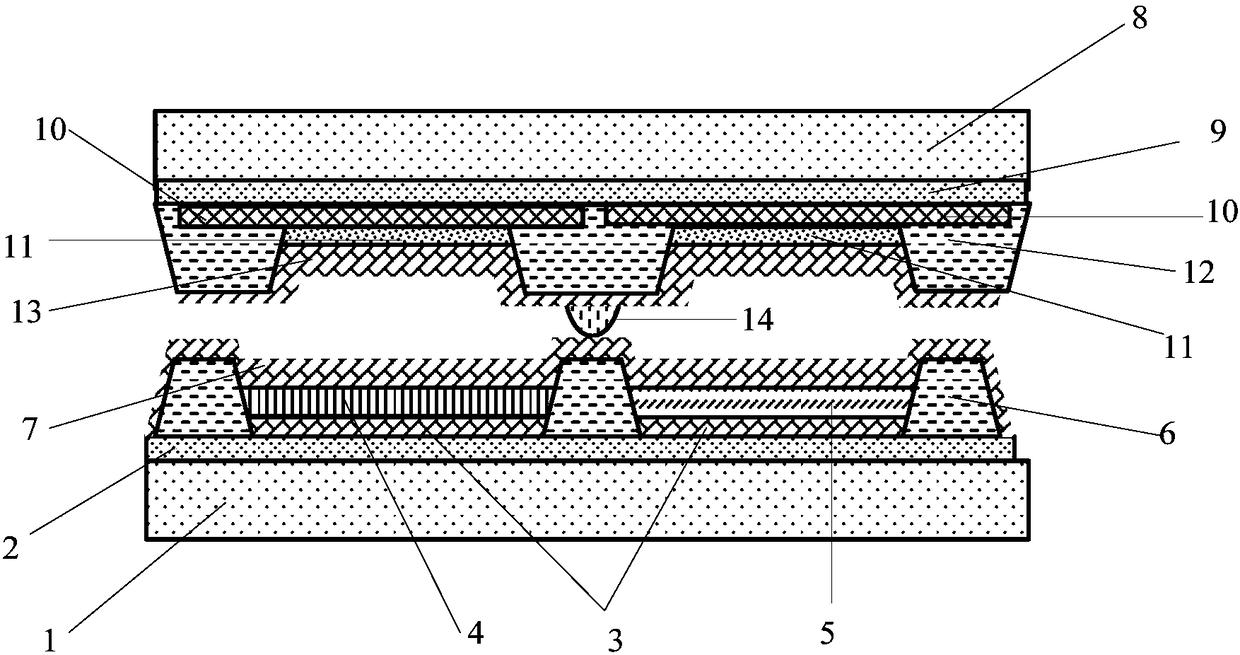
[0013] Please refer to figure 1 , this embodiment provides an OLED display panel, including a first substrate 1 and a second substrate 8 oppositely arranged, and at least one red sub-pixel 4 is arranged at intervals on the surface of the first substrate 1 close to the second substrate 8 and at le...


PUM


Abstract

The invention discloses an OLED display panel and a display. The OLED display panel comprises a first substrate and a second substrate, which are oppositely arranged; at least one red sub-pixel and atleast one green sub-pixel are arranged on the surface of the first substrate close to the second substrate at intervals; at least two blue sub-pixels are arranged on the surface of the second substrate close to the first substrate at intervals; and each red sub-pixel and each green sub-pixel are separately just aligned to a blue sub-pixel. According to the technical scheme provided in the embodiment of the invention, the red sub-pixel, the green sub-pixel and the blue sub-pixel are separately arranged on the two different substrates; the two substrates are oppositely arranged; therefore, theresolution required by each process is reduced; and furthermore, the layout space becomes large.

Description

technical field [0001] The present disclosure generally relates to the field of display panels, and more particularly, to OLED display panels and displays. Background technique [0002] Organic light-emitting diodes have broad application prospects due to their high color gamut, high efficiency, self-illumination characteristics for displays, easy large-area preparation, and full-color display, and have attracted widespread attention, especially for large-scale applications. size display applications. However, due to the increasingly high resolution requirements in the TV market, the aperture ratio of OLED (Organic Light-Emitting Diode, Organic Light-Emitting Diode) devices is considerably compressed, resulting in problems such as shorter device life and lower display brightness. In addition, the pixel gap of high-resolution products is narrow, which is not conducive to the use of printing technology, and the problem of color mixing often occurs due to the mixing of lumines...

Claims


Application Information

Patent Timeline
IPC IPC(8): H01L27/32
CPCH10K59/353H10K59/90H10K59/32H10K59/128H10K71/13H10K71/50H10K50/818H10K50/865H01L27/1218H10K50/156H10K50/828
Inventor 许名宏
Owner BOE TECH GRP CO LTD
Learn More