PCB electroplating device and using method

An electroplating device and PCB board technology, which is applied in the direction of plating tanks, electrolytic processes, electrolytic components, etc., can solve the problems of inconsistent coating thickness of plated parts, uneven plating of electroplated plates, etc., and achieve the effect of avoiding inconsistent coating thickness and ensuring quality

Inactive Publication Date: 2018-07-20
ANHUI DASHENG ELECTRONICS
View PDF4 Cites 0 Cited by
  • Summary
  • Abstract
  • Description
  • Claims
  • Application Information

AI Technical Summary

Problems solved by technology

[0002] Electroplating is an important process in the production process of PCB boards, but traditional electroplating devices often cause uneven plating of electroplated boards. For example, the power supply of some PCB electroplating devices is set on one side of the electroplating tank, and the cables connected to the power supply at both ends of the electroplating tank Different lengths will lead to inconsistent coating thickness of the plated parts, so we need to improve the existing electroplating device to reduce production costs and improve the uniformity of the electroplated layer on the electroplated parts, so as to achieve consistent coating thickness of the plated parts

Method used


Image

  • PCB electroplating device and using method
  • PCB electroplating device and using method

Examples


Embodiment Construction

[0021] The present invention will be further described below in conjunction with the accompanying drawings and specific embodiments. The following examples are intended to illustrate the present invention rather than further limit the present invention.

[0022] The technical scheme of concrete implementation of the present invention is:

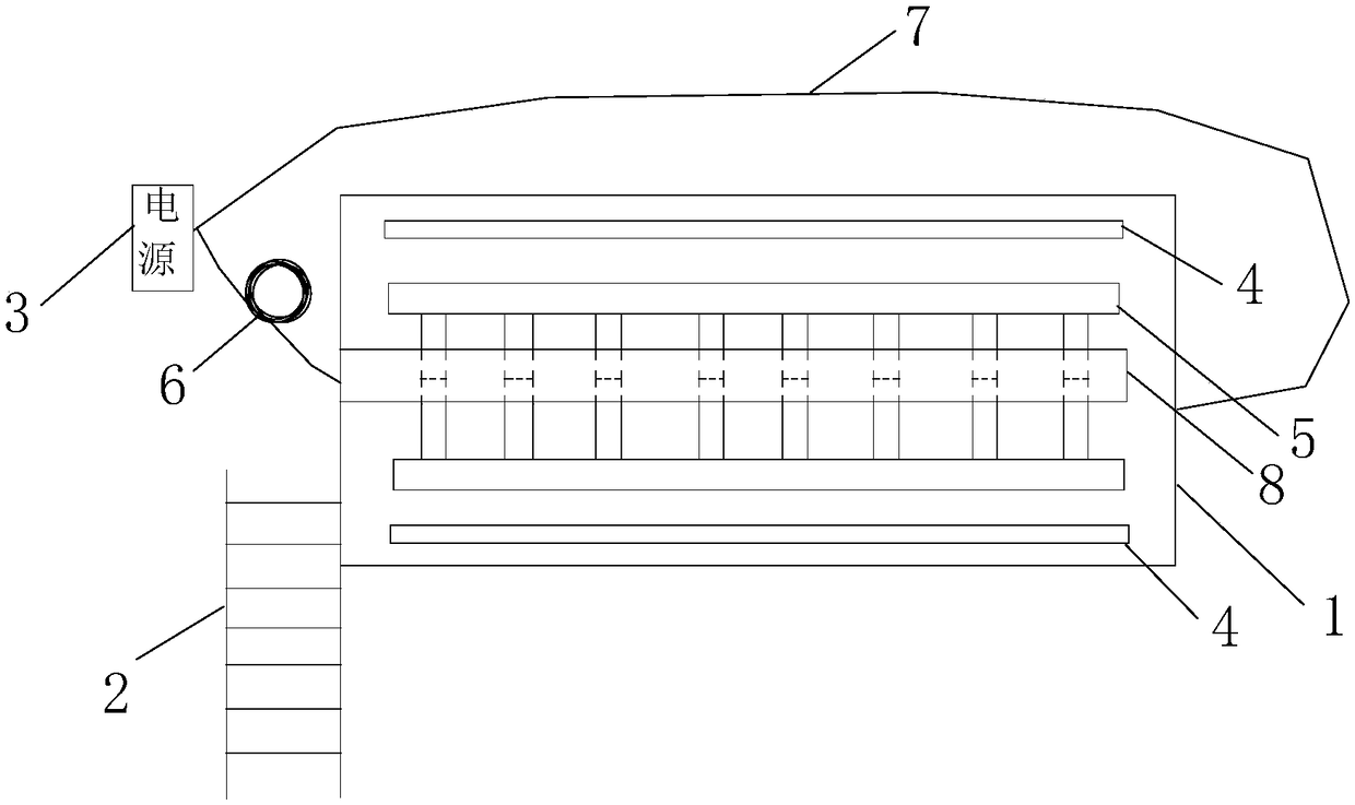
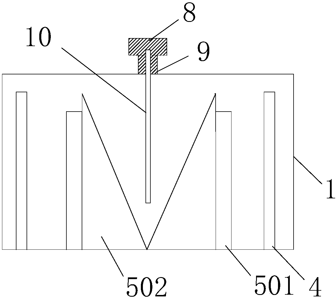
[0023] combine figure 1 with figure 2 as shown, figure 1 It is a top view of a PCB electroplating device according to an embodiment of the present invention, figure 2 It is a side view of an internal electroplating float frame of a PCB electroplating device according to an embodiment of the present invention. A PCB electroplating device of the present invention includes a plating solution cylinder 1, a walking bridge 2, a power supply 3, an electrode 4, an electroplating floating frame 5, a first cable 6 and a second cable 7, wherein the electroplating floating frame 5 includes a baffle 501 and supporting feet 502;

[0024] The walkin...


PUM


Abstract

The invention provides a PCB electroplating device which comprises a plating solution cylinder, a walking bridge arranged on one side of the plating solution cylinder and a power source connected withthe plating solution cylinder through cable wires. The device further comprises electrodes arranged on the two sides inside the plating solution cylinder and an electroplating scaffold located between the electrodes on the two sides. The two cable wires comprises the first cable wire and the second cable wire with the same length, wherein the first cable wire is connected to the portion, on one side of the walking bridge, of the plating solution cylinder, and the second cable wire is connected to the portion, on the other side of the walking bridge, of the plating solution cylinder. The electroplating scaffold comprises baffles on the two sides and supporting feet, wherein the baffles are parallel to the electrodes, and the supporting feet are connected with the baffles and located in themiddle of the plating solution cylinder. According to the PCB electroplating device, the production cost is reduced, the uniformity of an electroplating layer on an electroplated part is improved, and therefore thickness consistency of the electroplating layer on the electroplated part is achieved.

Description

technical field [0001] The invention relates to the technical field of circuit board production, in particular to a PCB electroplating device and a use method. Background technique [0002] Electroplating is an important process in the production process of PCB boards, but traditional electroplating devices often cause uneven plating of electroplated boards. For example, the power supply of some PCB electroplating devices is set on one side of the electroplating tank, and the cables connected to the power supply at both ends of the electroplating tank Different lengths will lead to inconsistent coating thickness of the plated parts, so we need to improve the existing electroplating device to reduce production costs and improve the uniformity of the electroplated layer on the electroplated parts, so as to achieve consistent coating thickness of the plated parts. Contents of the invention [0003] The technical problem to be solved by the present invention is to improve the ...

Claims


Application Information

Patent Timeline
Patent Type & Authority Applications(China)
IPC IPC(8): C25D17/02C25D17/08C25D7/00
CPCC25D17/02C25D7/00C25D17/08
Inventor 陈国康
Owner ANHUI DASHENG ELECTRONICS
Why Eureka
Try Eureka