
OLED array substrate, display device and method for repairing dark spots thereof

An array substrate and repair method technology, applied in the field of organic light-emitting diode array substrates, can solve problems such as dark spots, anode and cathode short circuits, damage to surrounding display areas, etc., to achieve the effect of eliminating bright spots and returning pixels to normal

Active Publication Date: 2019-12-03
BOE TECH GRP CO LTD +1
View PDF3 Cites 0 Cited by
  • Summary
  • Abstract
  • Description
  • Claims
  • Application Information

AI Technical Summary

Problems solved by technology

During the preparation of OLED display devices, residual impurities are likely to cause local short circuits between the anode and the cathode, resulting in dark spot defects.
During the use of OLED display devices, the size of dark spots may gradually increase, until finally the entire pixel unit becomes a dark pixel that cannot be lit, resulting in a decrease in the reliability of OLED display devices
Or, OLED display devices may have bright spot defects due to defects in components such as TFT (Thin Film Transistor) in the pixel structure (for example, a short circuit between the anode and the power line)
[0004] For dark spot defects, the conventional repair method is to use laser to remove impurities in the short-circuit area, but this method will damage the surrounding display area; for bright spot defects, the conventional repair method is to make backup lines on the array substrate, or cut off the Data lines, and then welding to connect the end of the TFT close to the OLED to a fixed potential, so that the cathode and anode of the OLED maintain the same potential to eliminate bright spot defects, but this method will occupy the wiring space, thereby affecting the aperture ratio

Method used


Image

  • OLED array substrate, display device and method for repairing dark spots thereof
  • OLED array substrate, display device and method for repairing dark spots thereof
  • OLED array substrate, display device and method for repairing dark spots thereof

Examples


Embodiment 1

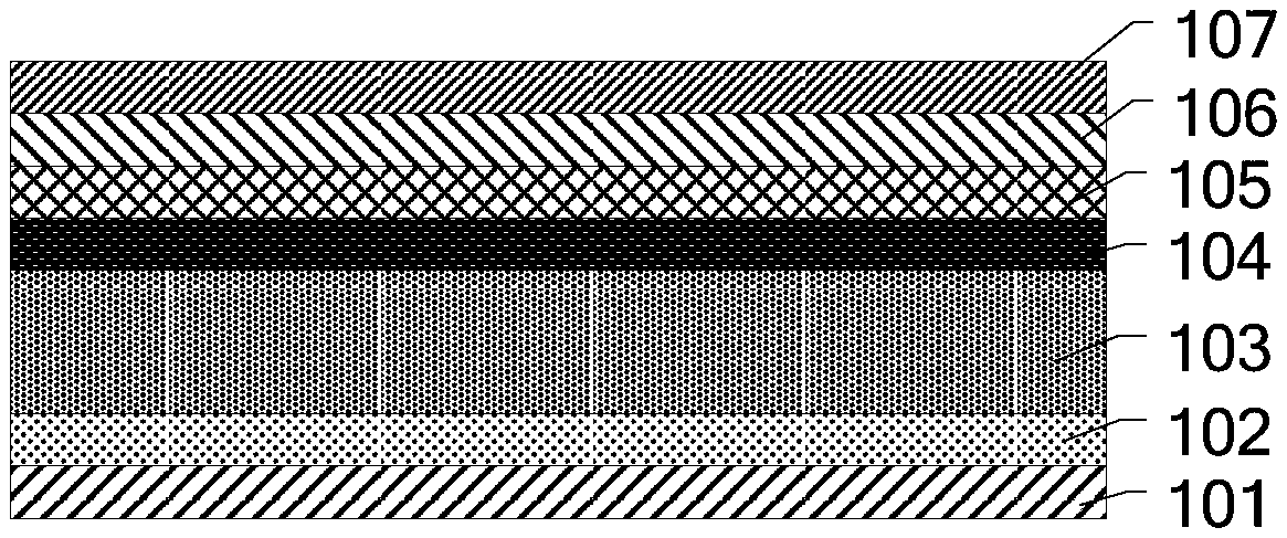
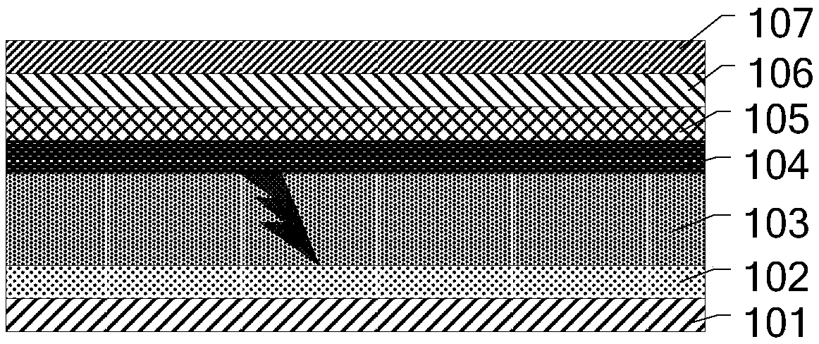
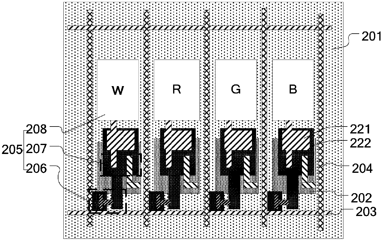
[0050] This embodiment provides an organic light emitting diode (OLED) array substrate, for example, image 3 A schematic plan view of an organic light emitting diode (OLED) array substrate provided in this embodiment, Figure 4a A schematic cross-sectional structure diagram of an organic light emitting diode (OLED) array substrate provided in this embodiment, Figure 4b A schematic cross-sectional structure diagram of another organic light emitting diode (OLED) array substrate provided in this embodiment.

[0051] Such as image 3 with Figure 4a , Figure 4b As shown, the OLED array substrate includes: a base substrate 201, a power line 202 arranged on the base substrate 201, a connecting part ( image 3 , Figure 4a with Figure 4b Not shown in ), gate line 203 and data line 204; pixel structure 205 arranged in the area defined by the intersection of gate line 203 and data line 204, pixel structure 205 includes switching transistor 206, driving transistor 207 and OLED...

Embodiment 2

[0086] This embodiment provides a display device, including any organic light emitting diode (OLED) array substrate in Embodiment 1, and may also include a gate drive circuit, a data drive circuit, and a power supply, etc., and the gate line is connected to the gate drive circuit. , the data line is connected to the data driving circuit, and the power wiring is connected to the power supply. The display device can be any product or component with a display function such as an OLED panel, a mobile phone, a tablet computer, a TV set, a monitor, a notebook computer, a digital photo frame, and a navigator.

[0087] The organic light emitting diode (OLED) array substrate included in the display device of this embodiment is the same as the above-mentioned Figure 4a , Figure 4b as well as Figure 4c Any one of the organic light emitting diode (OLED) array substrates shown has the same structure, and its technical effects and implementation principles are the same, and will not be...

Embodiment 3

[0090] This embodiment provides an organic light emitting diode (OLED) array substrate in the first embodiment and a method for repairing dark spots of the display device in the second embodiment, Figure 10 A flow chart of a method for repairing dark spots provided in this embodiment, such as Figure 10 Shown, this preparation method comprises the steps:

[0091] Step 101, electrically connecting the power line and the first electrode;

[0092] Step 102, applying a voltage to the first electrode through the power line so that the first electrode and the second electrode are no longer short-circuited;

[0093] Step 103, electrically isolating the power line and the first electrode.

[0094] For example, the first laser irradiation is performed on the connection part corresponding to the pixel structure to be repaired for laser welding, and the power line and the first electrode are welded by controlling the energy and time of laser irradiation to electrically connect the pow...


PUM


Abstract

The application provides an organic light emitting diode (OLED) array substrate, a display device and a method for repairing dark spots thereof. The OLED array substrate includes: a power supply line, a connecting part; a pixel structure arranged in the pixel area, the pixel structure includes a driving transistor and an OLED device, the connecting part has a first end and a second end, and the first end is connected to the second end of the OLED device. An electrode is electrically connected or arranged to be weldable with the first electrode, and the second terminal is electrically connected to the second source-drain electrode or the power supply line, or is arranged to be weldable with the second source-drain electrode or the power supply line of the drive transistor, and the connecting part The first electrode (anode or cathode) of the OLED device is electrically connected to the power supply line through the connecting part, and then the conductive foreign matter between the anode and the cathode of the OLED device is not electrically connected to the power line before welding. Burning is used to repair the dark spots of the display device. The dark spot repair method is easy to operate and will not cause adverse effects on peripheral circuits.

Description

technical field [0001] Embodiments of the present invention relate to an organic light emitting diode (OLED) array substrate, a display device and a method for repairing dark spots thereof. Background technique [0002] Organic light-emitting diode (OLED) display devices are active light-emitting devices. Compared with the mainstream thin film transistor liquid crystal display (Thin Film Transistor-Liquid Crystal Display, TFT-LCD), OLED devices have high contrast, wide viewing angle, low power consumption, light and thin OLED devices have received more and more attention due to their advantages. [0003] An OLED device includes an anode, a cathode, and a light emitting layer disposed between the anode and the cathode. When a voltage is applied between the anode and the cathode, holes and electrons move to the light-emitting layer, and the holes and electrons recombine in the light-emitting layer to emit light. During the preparation process of OLED display devices, residua...

Claims


Application Information

Patent Timeline
Patent Type & Authority Patents(China)
IPC IPC(8): H01L27/32H01L51/56
CPCH10K59/131H10K59/8052H10K59/8051H01L27/124H01L27/1255H10K59/351H10K59/1213H10K71/861H10K2102/341H10K50/81H10K50/82H10K59/123H10K71/00
Inventor 艾雨谢学武孙诗刘博文赵程鹏
Owner BOE TECH GRP CO LTD
Learn More