Organic light-emitting display panel and preparation method thereof

A technology of light-emitting display and organic light-emitting layer, which is applied in semiconductor/solid-state device manufacturing, electrical components, electrical solid-state devices, etc., can solve the problem of inability to balance pixel resolution and inkjet printing accuracy, and achieve the effect of improving pixel resolution

Inactive Publication Date: 2018-06-15
SOUTH CHINA UNIV OF TECH
View PDF2 Cites 10 Cited by
  • Summary
  • Abstract
  • Description
  • Claims
  • Application Information

AI Technical Summary

Problems solved by technology

[0005] In view of this, an embodiment of the present invention provides an organic light emitting display panel and a manufacturing method thereof, so as to solve the technical problem that the pixel resolution and inkjet printing accuracy of the organic light emitting display panel cannot be balanced in the prior art

Method used


Image

  • Organic light-emitting display panel and preparation method thereof
  • Organic light-emitting display panel and preparation method thereof
  • Organic light-emitting display panel and preparation method thereof

Examples


Embodiment Construction

[0052] In order to make the purpose, technical solution and advantages of the present invention clearer, the technical solution of the present invention will be fully described below through specific implementation in combination with the drawings in the embodiments of the present invention. Apparently, the described embodiments are some embodiments of the present invention, rather than all embodiments. Based on the embodiments of the present invention, all other embodiments obtained by persons of ordinary skill in the art without making creative efforts, All fall within the protection scope of the present invention.

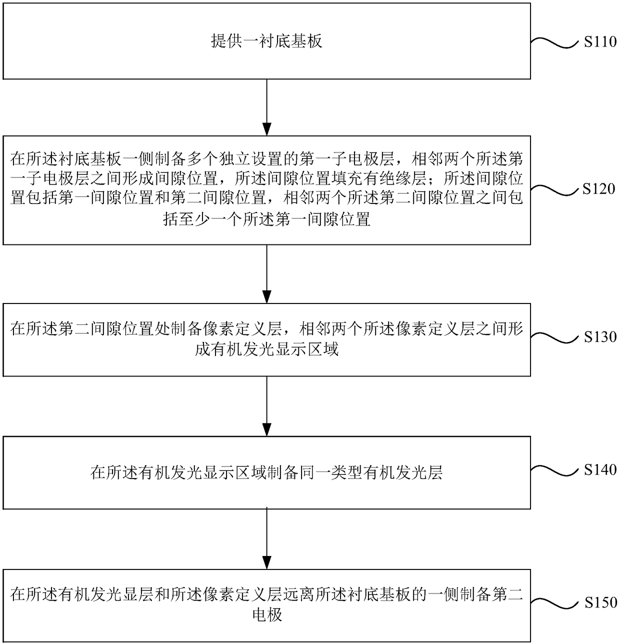
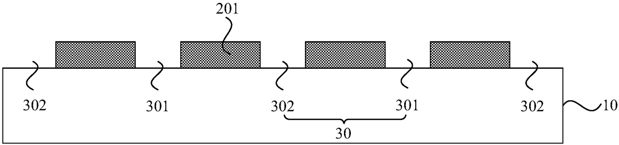
[0053] An embodiment of the present invention provides a method for manufacturing an organic light-emitting display panel, including providing a base substrate; preparing a plurality of independently arranged first sub-electrodes on one side of the base substrate, and forming a A gap position, the gap position is filled with an insulating layer; the gap position...


PUM


Abstract

The embodiments of the invention disclose an organic light-emitting display panel and a preparation method thereof. The preparation method of the organic light-emitting display panel comprises the following steps of: providing a substrate; preparing multiple independently-set first sub electrodes on one side of the substrate, wherein an interstitial site is formed between the adjacent two first sub electrodes, the interstitial site is filled with an insulation layer, each interstitial site comprises a first interstitial site and a second interstitial site, and the clearance between the adjacent two second interstitial sites comprises at least one first interstitial site; preparing pixel definition layers on the second interstitial site position, wherein an organic light-emitting display area is formed between two adjacent pixel definition layers; preparing the same type of organic light-emitting layers on the organic light-emitting display area; and preparing second electrodes on one sides, far from the substrate, of the organic light-emitting display layers and the pixel definition layers. In conclusion, the pixel resolution of the organic light-emitting display panel can be improved without changing the preparation process of the organic light-emitting layer in the existing organic light-emitting display panel.

Description

technical field [0001] Embodiments of the present invention relate to the field of semiconductor display technologies, and in particular to an organic light emitting display panel and a manufacturing method thereof. Background technique [0002] Organic Light-Emitting Diode (OLED) display device has self-illumination, low driving voltage, high luminous efficiency, short response time, high definition and contrast, nearly 180° viewing angle, wide operating temperature range, and can realize flexible display With many advantages of large-area full-color display lights, it is recognized as the display device with the most development potential in the industry. [0003] At this stage, OLED display devices based on the vacuum process have been mass-produced. However, the equipment investment and maintenance costs of this technology are high, material waste is serious, it is difficult to achieve a larger area, and the cost remains high. Inkjet printing technology to prepare OLED ...

Claims


Application Information

Patent Timeline
Patent Type & Authority Applications(China)
IPC IPC(8): H01L51/56H01L27/32
CPCH10K59/35H10K71/00
Inventor 邹建华王磊徐苗陶洪宁洪龙彭俊彪
Owner SOUTH CHINA UNIV OF TECH
Why Eureka
Try Eureka