Flip LED chip and manufacturing method thereof

A technology of LED chips and manufacturing methods, which is applied to electrical components, circuits, semiconductor devices, etc., can solve the problems of low external quantum efficiency, increase the total reflection area, improve external quantum efficiency and stability, and prevent falling off and fragmentation Effect

Pending Publication Date: 2018-06-15
FOSHAN NATIONSTAR SEMICON
View PDF9 Cites 5 Cited by
  • Summary
  • Abstract
  • Description
  • Claims
  • Application Information

AI Technical Summary

Problems solved by technology

At present, the internal quantum efficiency of LED chips has reached more than 90%, but the external quantum efficiency is relatively low.

Method used


Image

  • Flip LED chip and manufacturing method thereof
  • Flip LED chip and manufacturing method thereof
  • Flip LED chip and manufacturing method thereof

Examples


Embodiment Construction

[0028] In order to make the object, technical solution and advantages of the present invention clearer, the present invention will be further described in detail below in conjunction with the accompanying drawings.

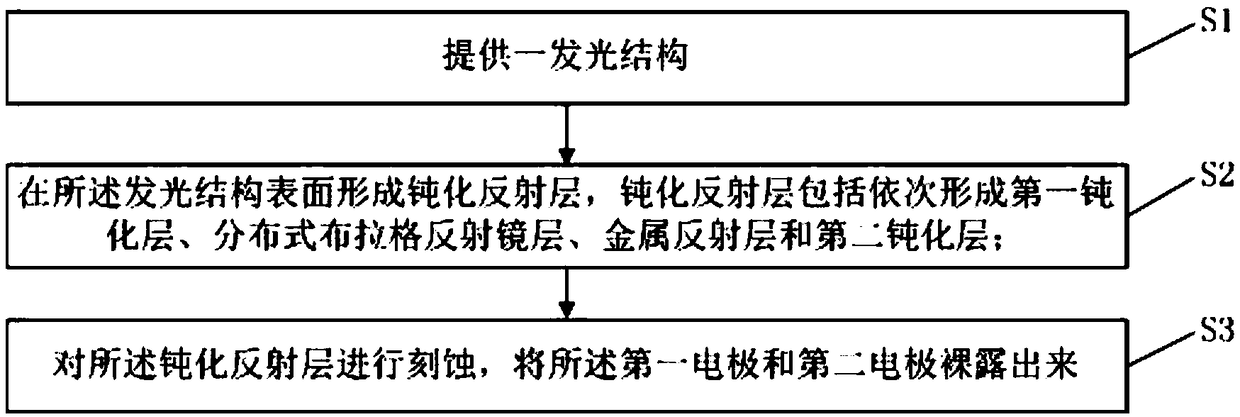
[0029] see figure 1 , figure 1 It is a flowchart of a manufacturing method of a flip-chip LED chip according to the present invention, wherein the manufacturing method of a flip-chip LED chip provided by the present invention includes the following steps:

[0030] S1: providing a light-emitting structure;

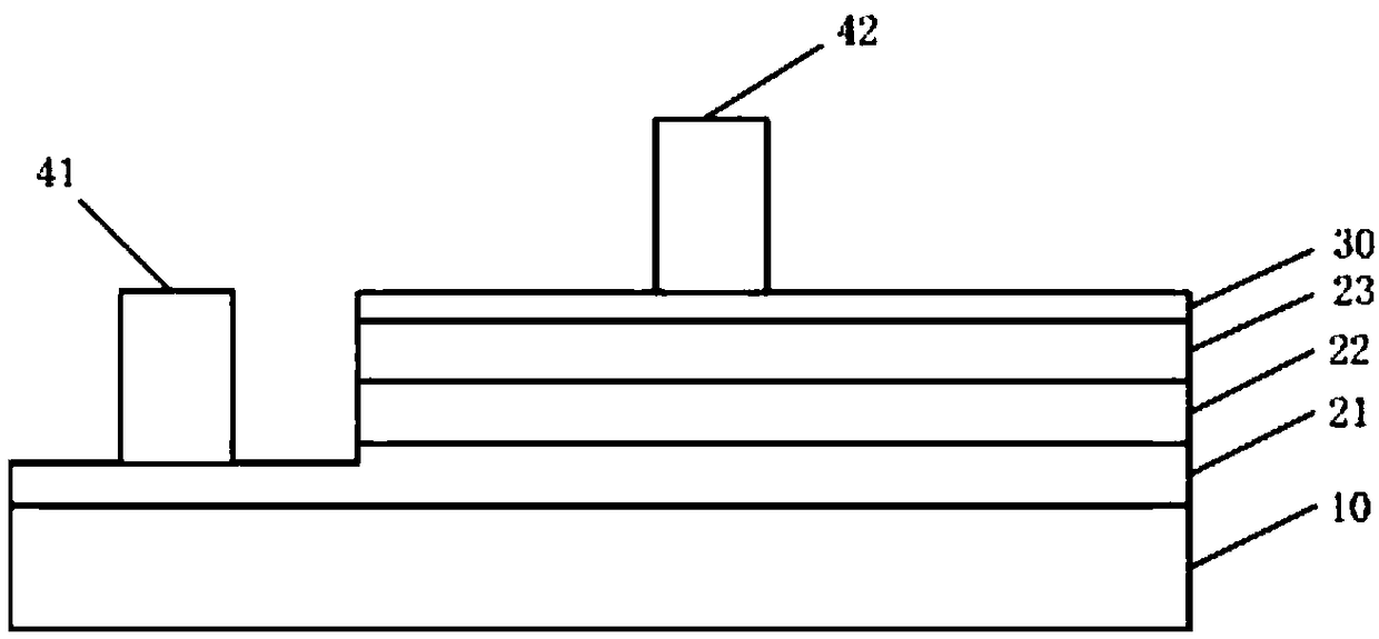
[0031] see Figure 2a , providing a light emitting structure, the light emitting structure includes a substrate 10, a first semiconductor layer 21 disposed on the surface of the substrate 10, an active layer 22 disposed on the surface of the first semiconductor layer 21 and a first electrode 41, disposed on the The second semiconductor layer 23 on the surface of the source layer 22 , the transparent conductive layer 30 on the surface of the second semiconduc...


PUM


Abstract

The invention discloses a manufacturing method of a flip LED (Light Emitting Diode) chip. The manufacturing method of a flip LED chip includes the steps: providing a light emitting structure; forminga passivation reflecting layer on the surface of the light emitting structure, wherein the passivation reflecting layer includes a first passivation layer, a distributed Bragg reflector layer, a metalreflection layer and a second passivation layer successively; and etching the passivation reflecting layer, and exposing a first electrode and a second electrode. In the manufacturing method of a flip LED chip, through coordination between the distributed Bragg reflector layer and the metal reflection layer, as the light emitted from an active layer is partially reflected by the distributed Braggreflector layer and then is totally reflected by the metal reflection layer again, electric leakage caused by the metal reflection layer can be avoided and the total reflection area is increased at the same time, thus effectively improving the external quantum efficiency and stability of the chip and increasing the chip brightness.

Description

technical field [0001] The invention relates to the technical field of light emitting diodes, in particular to a flip-chip LED chip and a manufacturing method thereof. Background technique [0002] LED (Light Emitting Diode, Light Emitting Diode) is a semiconductor device that uses carrier recombination to release energy to form light. LED chips have low power consumption, pure chromaticity, long life, small size, fast response time, energy saving and environmental protection, etc. Many advantages. [0003] The luminous efficiency of LED chips is mainly determined by internal quantum efficiency and external quantum efficiency. At present, the internal quantum efficiency of LED chips has reached more than 90%, but the external quantum efficiency is relatively low. Therefore, how to improve the external quantum efficiency of LED chips has become a key research direction in the industry. Contents of the invention [0004] The technical problem to be solved by the present i...

Claims


Application Information

Patent Timeline
Patent Type & Authority Applications(China)
IPC IPC(8): H01L33/46H01L33/00
CPCH01L33/0075H01L33/46H01L2933/0025
Inventor 王兵李治葵
Owner FOSHAN NATIONSTAR SEMICON
Why Eureka
Try Eureka