Eureka AIR delivers breakthrough ideas for toughest innovation challenges, trusted by R&D personnel around the world.

Detection marking device and detection marking method of circuit board

A technology for marking equipment and circuit boards, which is applied to welding equipment, laser welding equipment, metal processing equipment, etc., can solve the problems of affecting the quality of circuit boards, low work efficiency, and prone to errors, etc., to reduce the number of transfers and structure Simplicity and the effect of reducing working hours

Pending Publication Date: 2018-06-12
东莞市科佳电路有限公司
View PDF5 Cites 5 Cited by
  • Summary
  • Abstract
  • Description
  • Claims
  • Application Information

AI Technical Summary

Problems solved by technology

[0002] In flexible circuit boards, it is often necessary to reinforce the circuit board with steel sheets. When the steel sheet is attached to the circuit board, the steel sheet is likely to be missed. When the circuit board is missing the steel sheet, it will affect the circuit board. Quality, at present, is to detect whether the missing steel sheet of the circuit board is detected by human eyes. If the position of the missing steel sheet is found, the position of the missing steel sheet is manually marked. This work is all done manually. , easy to make mistakes, and its work efficiency is low. After manually detecting the missing steel sheet, it is necessary to write down the position of the missing steel sheet, and then transfer it to another worker for marking. Transferring is time-consuming and labor-intensive

Method used


Image

  • Detection marking device and detection marking method of circuit board
  • Detection marking device and detection marking method of circuit board
  • Detection marking device and detection marking method of circuit board

Examples


Embodiment Construction

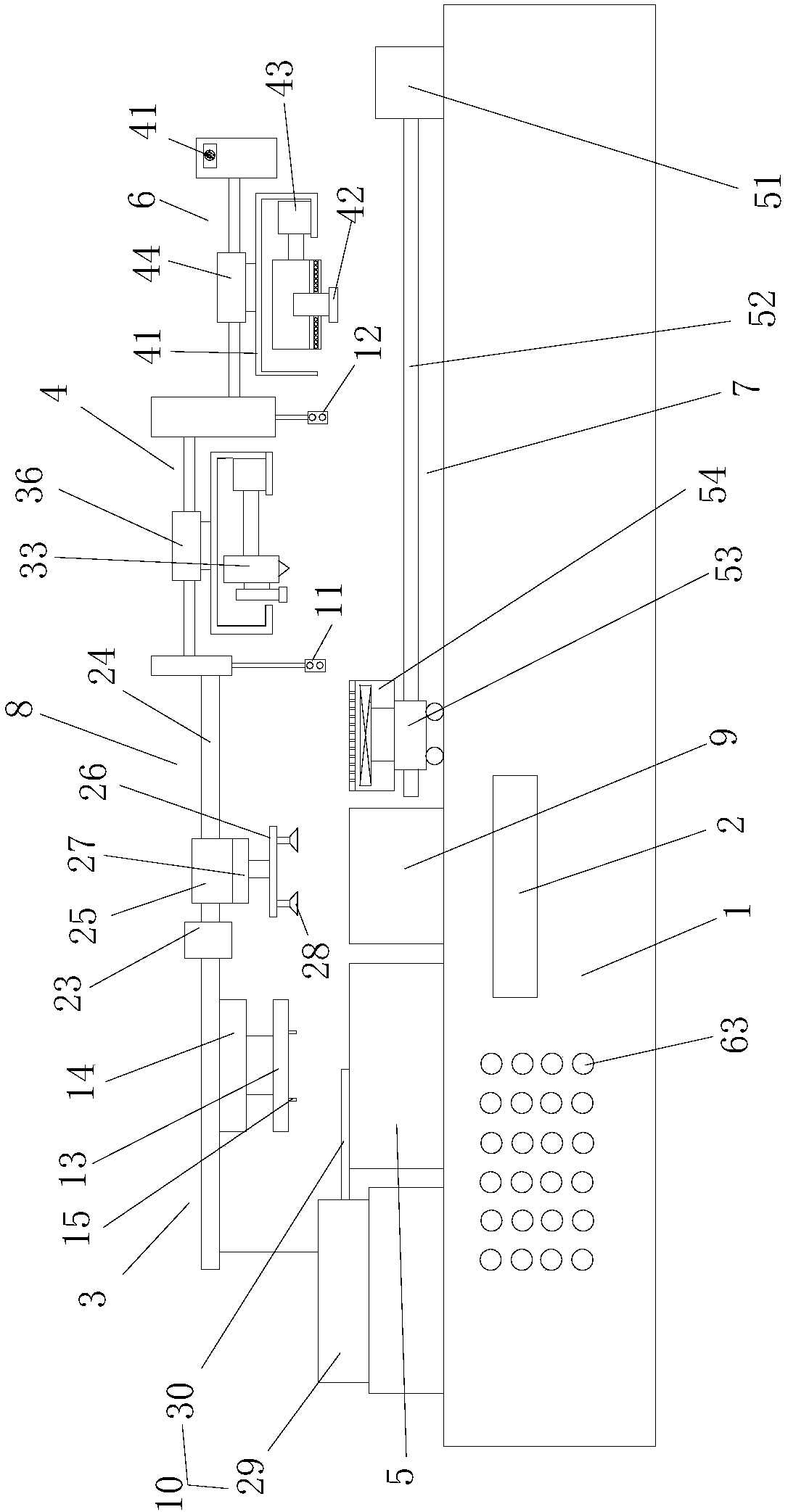
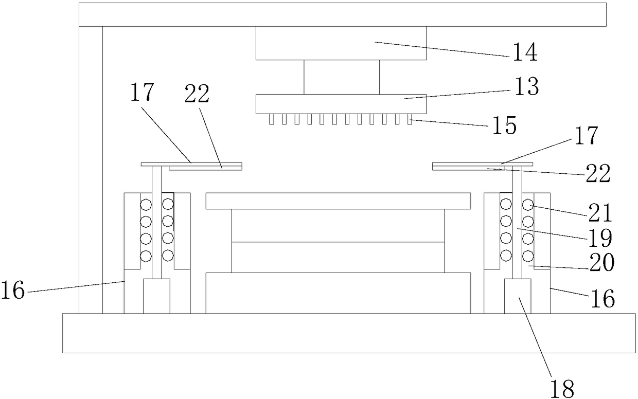
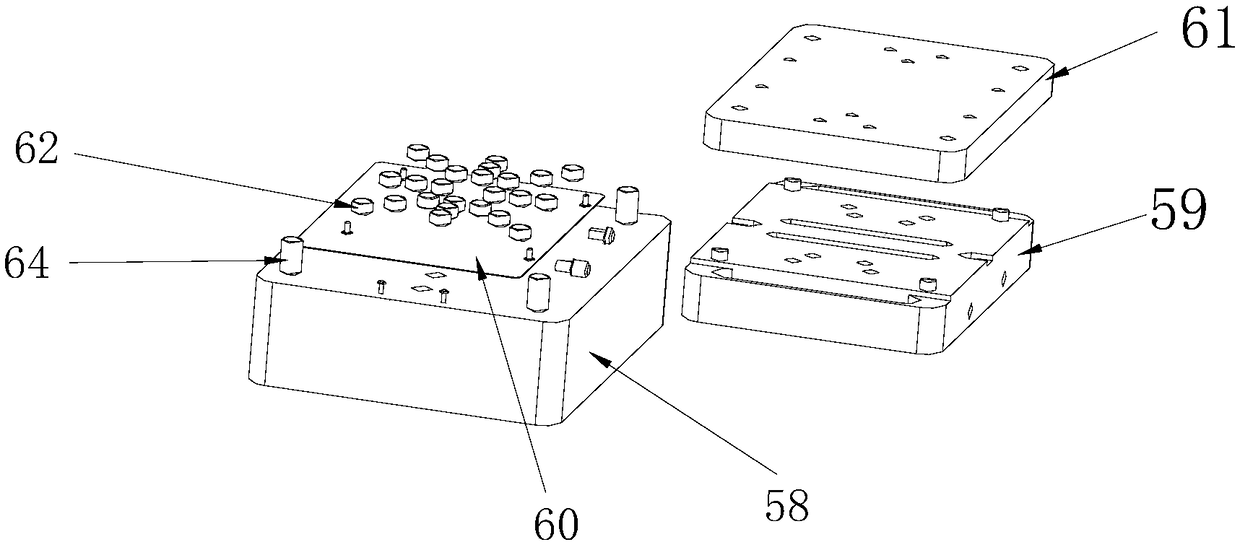
[0062] In order to facilitate the understanding of those skilled in the art, the present invention will be further described below in conjunction with the embodiments and accompanying drawings, and the contents mentioned in the embodiments are not intended to limit the present invention. The present invention will be described in detail below in conjunction with the accompanying drawings.

[0063] Such as figure 1 As shown, a circuit board detection and marking device described in this embodiment includes a frame 1 and a controller 2, and the frame 1 is sequentially provided with detection devices for detecting missing steel sheets on the circuit board. Device 3, a marking device 4 for laser marking circuit boards and an appearance inspection device 6 for visual inspection of circuit boards; a material transfer device is installed below the marking device 4 and the appearance inspection device 6 7. A transfer device 8 for transferring the circuit board from the detection devi...


PUM


Abstract

The invention relates to the technical field of processing of a circuit board, in particular to a detection marking device and detection marking method of a circuit board. The detection marking devicecomprises a stander and a controller, wherein the stander is successively provided with a detection apparatus for detecting the missing of a steel sheet of the circuit board, a marking apparatus forlaser marking the circuit board and an appearance examination apparatus for examining the appearance of the circuit board; a material moving apparatus is installed below the marking apparatus and theappearance examining apparatus, and a transferring apparatus for transferring the circuit board from the detection apparatus to the material transferring apparatus is arranged between the detection apparatus and the marking apparatus; one side of the detection apparatus is provided with a receiving seat, and the other side of the detection apparatus is provided with a pushing apparatus for pushingthe circuit board to the receiving seat; and a first sensor is arranged between the marking apparatus and the transferring apparatus. The detection marking device is simple in structure, reasonable in design, capable of realizing the streamline operation of the detection, marking and appearance examination, capable of increasing the working efficiency and reducing the carrying transferring times,and time-saving and labor-saving.

Description

technical field [0001] The invention relates to the technical field of circuit board processing, in particular to a circuit board detection and marking device and a detection and marking method thereof. Background technique [0002] In flexible circuit boards, it is often necessary to reinforce the circuit board with steel sheets. When the steel sheet is attached to the circuit board, the steel sheet is likely to be missed. When the circuit board is missing the steel sheet, it will affect the circuit board. Quality, at present, is to detect whether the missing steel sheet of the circuit board is detected by human eyes. If the position of the missing steel sheet is found, the position of the missing steel sheet is manually marked. This work is all done manually. , easy to make mistakes, and its work efficiency is low. After manually detecting the missing steel sheet, it is necessary to write down the position of the missing steel sheet, and then transfer it to another worker ...

Claims


Application Information

Patent Timeline
Patent Type & Authority Applications(China)
IPC IPC(8): G01N21/956G01V3/00B23K26/362
CPCG01N21/956G01V3/00B23K26/361G01N2021/95638
Inventor 徐承升廖发盆陈军民李才文夏军
Owner 东莞市科佳电路有限公司
Why Eureka
Eureka Blog
Learn More