Chip bonding device and chip bonding method

A chip bonding and chip technology, applied in the direction of electrical components, semiconductor/solid-state device manufacturing, circuits, etc., can solve time-consuming and labor-intensive problems

Active Publication Date: 2018-06-05
SHANGHAI MICRO ELECTRONICS EQUIP (GRP) CO LTD
View PDF4 Cites 3 Cited by
  • Summary
  • Abstract
  • Description
  • Claims
  • Application Information

AI Technical Summary

Problems solved by technology

This kind of chip bonding equipment and bonding method requires repeated actions for each chip, which is time-consuming and laborious.

Method used


Image

  • Chip bonding device and chip bonding method
  • Chip bonding device and chip bonding method
  • Chip bonding device and chip bonding method

Examples


Embodiment Construction

[0048] In order to make the above objects, features and advantages of the present invention more comprehensible, specific implementations of the present invention will be described in detail below in conjunction with the accompanying drawings.

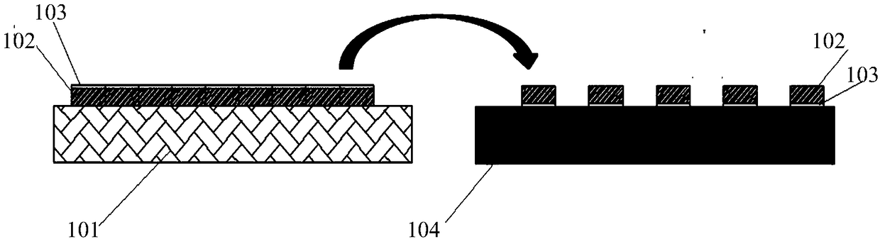
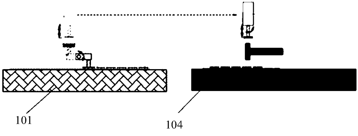
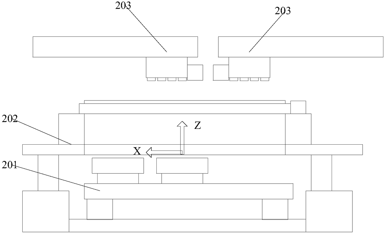
[0049] Please refer to image 3 , with the horizontal direction as the X direction, the vertical direction perpendicular to the horizontal plane as the Z direction, and the plane formed perpendicular to the X and Z directions as the Y direction, an XYZ three-dimensional coordinate system is established. The invention provides a chip bonding device, which includes from top to bottom

[0050] There are several batches of chip transfer parts 203 , substrate carrying parts 202 and bonding force output parts 201 .

[0051] Specifically, several groups of batch chip transfer components 203 are arranged in six groups in this embodiment, forming two columns respectively, as Figure 5 As shown, the first to third batches of chip transmission ...


PUM


Abstract

The invention provides a chip bonding device and a chip bonding method. The chip bonding device comprises a plurality of groups of batch chip transmission parts, a base bearing part and a bonding force output part from top to bottom. In the chip bonding device and the chip bonding method provided in the invention, the batch chip transmission part can bond several chips at one time, the chips are bonded to a base borne by the base bearing part at the same time; in the case of bonding, a bonding ejection mechanism only needs to be used to eject the base bearing part until the base on the base bearing part is bonded with a plurality of chips, that is, only one mechanism is needed to perform a vertical movement in the case of bonding, the movement path and steps are simplified, the productionefficiency is improved, the time is saved, and mass production demands can be met.

Description

technical field [0001] The invention relates to the field of semiconductor manufacturing, in particular to a chip bonding device and a chip bonding method. Background technique [0002] Die bonding is a form of interconnection formed by connecting a chip to a carrier. Such as figure 1 with figure 2 Shown is a schematic diagram of the chip bonding process. The pre-bonded chip 102 is placed on the separation table 101 with the marking surface 103 facing upwards, and the pre-bonded chip 102 is transferred to the substrate 104 by grabbing and flipping the robot. [0003] The known chip bonding equipment picks up a single chip from the source through a suction head that matches the size of the chip, and then aligns the chip with the alignment mark of the carrier through a machine alignment system, and then directly presses the chip combined to form interconnects on the substrate. This kind of chip bonding equipment and bonding method requires repeated actions for each chip, ...

Claims


Application Information

Patent Timeline
Patent Type & Authority Applications(China)
IPC IPC(8): H01L21/56H01L21/67
Inventor 姜晓玉余斌夏海
Owner SHANGHAI MICRO ELECTRONICS EQUIP (GRP) CO LTD
Why Eureka
Try Eureka