
Avalanche multiplier bi-directional scan tdiccd

An avalanche multiplication and two-way scanning technology, which is applied in the field of TDICCD, can solve the problem that the performance is difficult to meet the high-speed simultaneous low-light imaging requirements, and achieve the effects of meeting special application requirements, improving imaging quality, and high signal-to-noise ratio

Active Publication Date: 2020-05-05
THE 44TH INST OF CHINA ELECTRONICS TECH GROUP CORP
View PDF8 Cites 0 Cited by
  • Summary
  • Abstract
  • Description
  • Claims
  • Application Information

AI Technical Summary

Problems solved by technology

The performance of the current TDICCD is difficult to meet the requirements of high-speed simultaneous low-light imaging

Method used


Image

  • Avalanche multiplier bi-directional scan tdiccd
  • Avalanche multiplier bi-directional scan tdiccd
  • Avalanche multiplier bi-directional scan tdiccd

Examples


Embodiment Construction

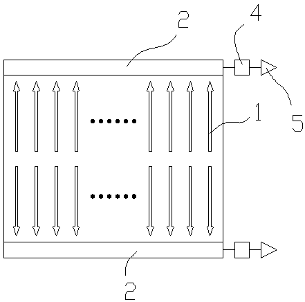
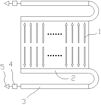
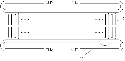
[0013] An avalanche multiplication bidirectional scanning TDICCD, the innovation of which is that the avalanche multiplication bidirectional scanning TDICCD includes a pixel array, a plurality of charge transfer channels 1, two horizontal transfer regions 2, a plurality of avalanche multiplication regions 3 and a plurality of Output structure; the pixel array is composed of a plurality of pixels, the upper edge of the pixel array forms the upper output side, and the lower edge of the pixel array forms the lower output side; the plurality of charge transfer channels 1 are arranged on In the pixel array, the two ends of the charge transfer channel 1 are respectively opposite to the upper output side and the lower output side; the first horizontal transfer area 2 is arranged at the position corresponding to the upper output side, and the second horizontal transfer area 2 is arranged At the position corresponding to the lower output side, the two ends of the charge transfer channel...


PUM


Abstract

The invention discloses an avalanche multiplication type bidirectional scanning TDICCD. The avalanche multiplication type bidirectional scanning TDICCD includes a pixel array, a plurality of charge transfer channels, two horizontal transfer regions, a plurality of avalanche multiplication regions and a plurality of output structures. The beneficial technical effects of the invention are as follows: the avalanche multiplication type bidirectional scanning TDICCD is proposed, and the device has a high signal-to-noise ratio, can greatly improve the imaging quality, and can meet special application requirements.

Description

technical field [0001] The invention relates to a TDICCD, in particular to an avalanche multiplying bidirectional scanning TDICCD. Background technique [0002] Charge Coupled Devices (CCD) is a solid-state semiconductor imaging device that uses the principle of charge coupling. The basic structure of CCD is an adjacent metal-oxide-semiconductor (Metal OxideSemiconductor, MOS) structure. In the semiconductor, photogenerated charges will be generated inside the semiconductor. When adjacent MOS structures are close to each other, if a voltage with a suitable timing is applied to the MOS electrodes, the charges can be stored and transferred in the MOS structure, and finally the photogenerated charge transfer In the signal readout area, the charge is converted into a voltage signal and the signal is amplified for subsequent signal processing. Compared with traditional imaging devices (such as vacuum imaging tubes, pyroelectric tubes, and silicon imaging tubes, etc.), CCD has ma...

Claims


Application Information

Patent Timeline
Patent Type & Authority Patents(China)
IPC IPC(8): H01L27/148
CPCH01L27/14812H01L27/14825
Inventor 王廷栋刘昌林白雪平
Owner THE 44TH INST OF CHINA ELECTRONICS TECH GROUP CORP
Learn More