Preparation method of VO2 thin film composite structure for near-infrared multi-band absorber
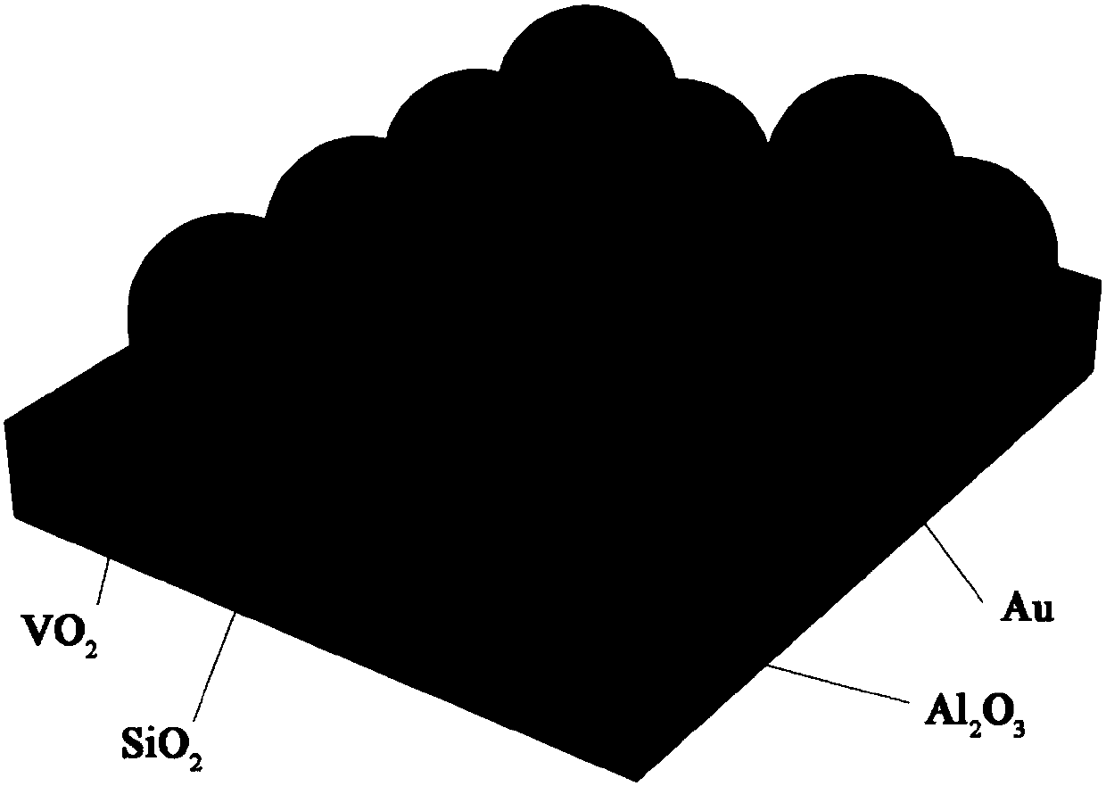
A composite structure and absorber technology, which is applied in the field of VO2 thin film composite structure preparation of near-infrared multi-broadband absorbers, can solve problems such as narrow absorption spectrum and absorption rate attenuation, achieve simple operation, high production efficiency, and realize multi-broadband absorption. Effect
- Summary
- Abstract
- Description
- Claims
- Application Information
AI Technical Summary
Problems solved by technology
Method used
Image
Examples
Embodiment 1
[0026] (1) Substrate cleaning:
[0027] The aluminum oxide substrate used is double-polished sapphire with (001) crystal plane, with a size of 1×1cm 2 , The thickness is 0.45mm. Put the substrate in deionized water, acetone, and absolute ethanol in order to ultrasonically clean it for 20 minutes to remove organic impurities on the surface; then wash it with deionized water, and finally put the substrate in absolute ethanol for later use.
[0028] (2) Evaporate and sputter gold film to prepare gold reflection layer:
[0029] A 100nm gold thin film was evaporated and sputtered on the cleaned substrate.
[0030] (3) Preparation of monodisperse SiO 2 mask layer:
[0031] First, insert the cleaned drain piece obliquely into deionized water, and then use a pipette gun to dissolve SiO with a particle size of 600nm 2 The ball solution is added dropwise to the drainage sheet, and it slowly flows to the water surface, and spreads evenly to form a high-density, large-area single-lay...
Embodiment 2
[0040] (1) Substrate cleaning:
[0041] The aluminum oxide substrate used is double-polished sapphire with (001) crystal plane, with a size of 1×1cm 2, The thickness is 0.45mm. Put the substrate in deionized water, acetone, and absolute ethanol in order to ultrasonically clean it for 30 minutes to remove organic impurities on the surface; then wash it with deionized water, and finally put the substrate in absolute ethanol for later use.
[0042] (2) Evaporate and sputter gold film to prepare gold reflection layer:
[0043] A 100nm gold thin film was evaporated and sputtered on the cleaned substrate.
[0044] (3) Preparation of monodisperse SiO 2 mask layer:
[0045] First, insert the cleaned drain piece obliquely into deionized water, and then use a pipette gun to dissolve SiO with a particle size of 600nm 2 The ball solution is added dropwise to the drainage sheet, and it slowly flows to the water surface, and spreads evenly to form a high-density, large-area single-laye...
Embodiment 3
[0051] (1) Substrate cleaning:
[0052] The aluminum oxide substrate used is double-polished sapphire with (001) crystal plane, with a size of 1×1cm 2 , The thickness is 0.45mm. Put the substrate in deionized water, acetone, and absolute ethanol in order to ultrasonically clean it for 30 minutes to remove organic impurities on the surface; then wash it with deionized water, and finally put the substrate in absolute ethanol for later use.
[0053] (2) Evaporate and sputter gold film to prepare gold reflection layer:
[0054] A 100nm gold thin film was evaporated and sputtered on the cleaned substrate.
[0055] (3) Preparation of monodisperse SiO 2 mask layer:
[0056] First, insert the cleaned drain piece obliquely into deionized water, and then use a pipette gun to dissolve SiO with a particle size of 600nm 2 The ball solution is added dropwise to the drainage sheet, and it slowly flows to the water surface, and spreads evenly to form a high-density, large-area single-lay...
PUM
| Property | Measurement | Unit |
|---|---|---|
| thickness | aaaaa | aaaaa |
| particle diameter | aaaaa | aaaaa |
Abstract
Description
Claims
Application Information
 - Generate Ideas
- Intellectual Property
- Life Sciences
- Materials
- Tech Scout
- Unparalleled Data Quality
- Higher Quality Content
- 60% Fewer Hallucinations
Browse by: Latest US Patents, China's latest patents, Technical Efficacy Thesaurus, Application Domain, Technology Topic, Popular Technical Reports.
© 2025 PatSnap. All rights reserved.Legal|Privacy policy|Modern Slavery Act Transparency Statement|Sitemap|About US| Contact US: help@patsnap.com


