Robotic Arms for Wafer Inspection

A robotic arm and wafer technology, applied in the manufacturing of electrical components, circuits, semiconductors/solid-state devices, etc., can solve problems such as increasing scrap rate, reducing production efficiency, waste of resources, etc., and achieving the effect of reducing scrap rate and improving production efficiency

Active Publication Date: 2020-07-10
YANGTZE MEMORY TECH CO LTD
View PDF11 Cites 0 Cited by
  • Summary
  • Abstract
  • Description
  • Claims
  • Application Information

AI Technical Summary

Problems solved by technology

The robotic arm is only used for wafer clamping and transportation. When the wafer is damaged in the acid bath solution and there are broken wafers left in the acid bath solution, the residual cannot be detected and the relative operation will be notified. Personnel stop the post-order operation of the wafer
When other batches of wafers are put into the acid tank solution containing residual wafer fragments again, the residual wafer fragments can cause extrusion damage to the re-introduced wafers, resulting in unnecessary waste of resources and increased waste. rate, reducing production efficiency

Method used


Image

  • Robotic Arms for Wafer Inspection
  • Robotic Arms for Wafer Inspection
  • Robotic Arms for Wafer Inspection

Examples


Embodiment Construction

[0022] Exemplary embodiments of the present disclosure will be described in more detail below with reference to the accompanying drawings. Although exemplary embodiments of the present disclosure are shown in the drawings, it should be understood that the present disclosure may be embodied in various forms and should not be limited by the embodiments set forth herein. Rather, these embodiments are provided for more thorough understanding of the present disclosure and to fully convey the scope of the present disclosure to those skilled in the art.

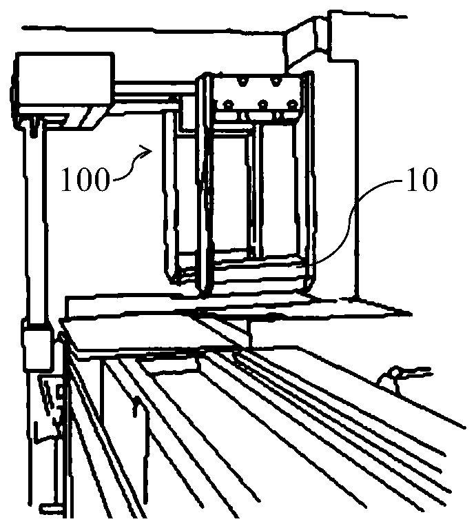
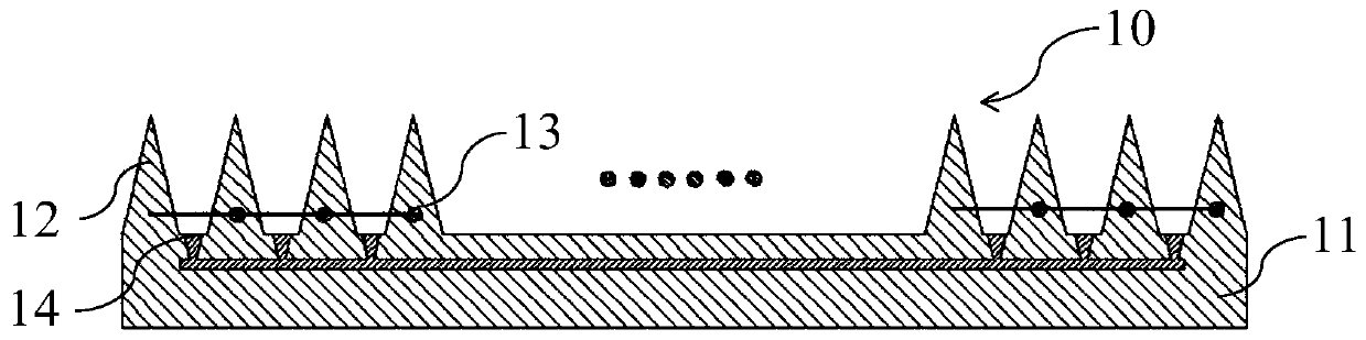
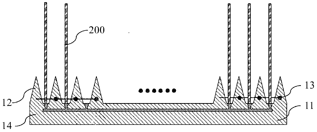
[0023] figure 1 It is a schematic diagram of the overall structure during the process of transporting wafers by the robot arm according to the embodiment of the present invention. figure 2 for figure 1 Schematic diagram of the cross-sectional structure of the wafer holder in the embodiment. image 3 for figure 2 The relationship between the position of the wafer holder and the wafer in the middle. As shown in the figure, the ...


PUM


Abstract

The invention belongs to the technical field of a semiconductor, and particularly relates to a mechanical arm for wafer detection. The mechanical arm for wafer detection comprises wafer fixing bases;the wafer fixing bases are arranged at both sides of the mechanical arm, and the wafer fixing bases at both sides of the mechanical arm are commonly used for fixing and supporting a wafer; a detectingunit for detecting a broken wafer is arranged on the wafer fixing base at one side of both sides of the mechanical arm. Through using the mechanical arm for wafer detection, the breakage of the wafercan be timely and effectively detected by arranging the detecting unit on the wafer fixing base, thereby preventing the residue of the broken wafer from extruding and damaging the next batch in an acid slot, reducing the rejection rate and improving the production efficiency.

Description

technical field [0001] The invention belongs to the technical field of semiconductors, and in particular relates to a mechanical arm for wafer detection. Background technique [0002] During the wafer etching process, it is often necessary to soak the wafer through multiple channels of acid bath solution to meet the requirements of the wafer surface quality. In the prior art, there is no relevant detection equipment for detecting wafer breakage in the acid bath solution. The robotic arm is only used for wafer clamping and transportation. When the wafer is damaged in the acid bath solution and there are broken wafers left in the acid bath solution, the residual cannot be detected and the relative operation will be notified. Personnel stop the subsequent operations of the wafer. When other batches of wafers are put into the acid tank solution containing residual wafer fragments again, the residual wafer fragments can cause extrusion damage to the re-introduced wafers, result...

Claims


Application Information

Patent Timeline
Patent Type & Authority Patents(China)
IPC IPC(8): H01L21/67
CPCH01L21/67288
Inventor 吴良辉蒋阳波张静平汪亚军顾立勋
Owner YANGTZE MEMORY TECH CO LTD
Why Eureka
Try Eureka