


Quick Research
Generate reliable direction feasibility study reports for your R&D in just a few steps.

Technical Q&A
Discover and master advanced knowledge NOW. Basics, ideas, possibilities, all at once.

Find Solutions
As an expert in R&D theories, this can generate solutions to your technical problems instantly.

Evaluate Feasibility
Analyze your overall solution with one click, know your potential R&D risks in advance.

Monitor Landscape
Get weekly tech updates, stay abreast of the latest tech innovations and key insights.
Chip packaging structure and method of integrated passive element
A chip packaging structure and passive component technology, applied in electrical components, electrical solid devices, semiconductor devices, etc., can solve the problems of low integration and large thickness of semiconductor packaging components, and achieve improved heat dissipation performance, high stability, and reliable coupling. high sex effect
- Summary
- Abstract
- Description
- Claims
- Application Information
AI Technical Summary
Problems solved by technology
Method used
Image

Examples
Embodiment 1
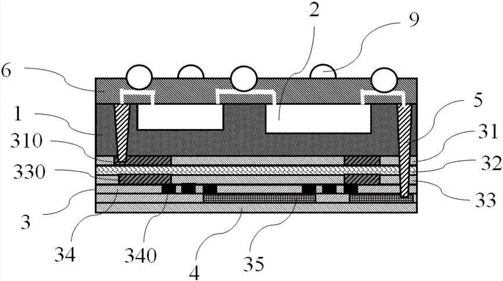
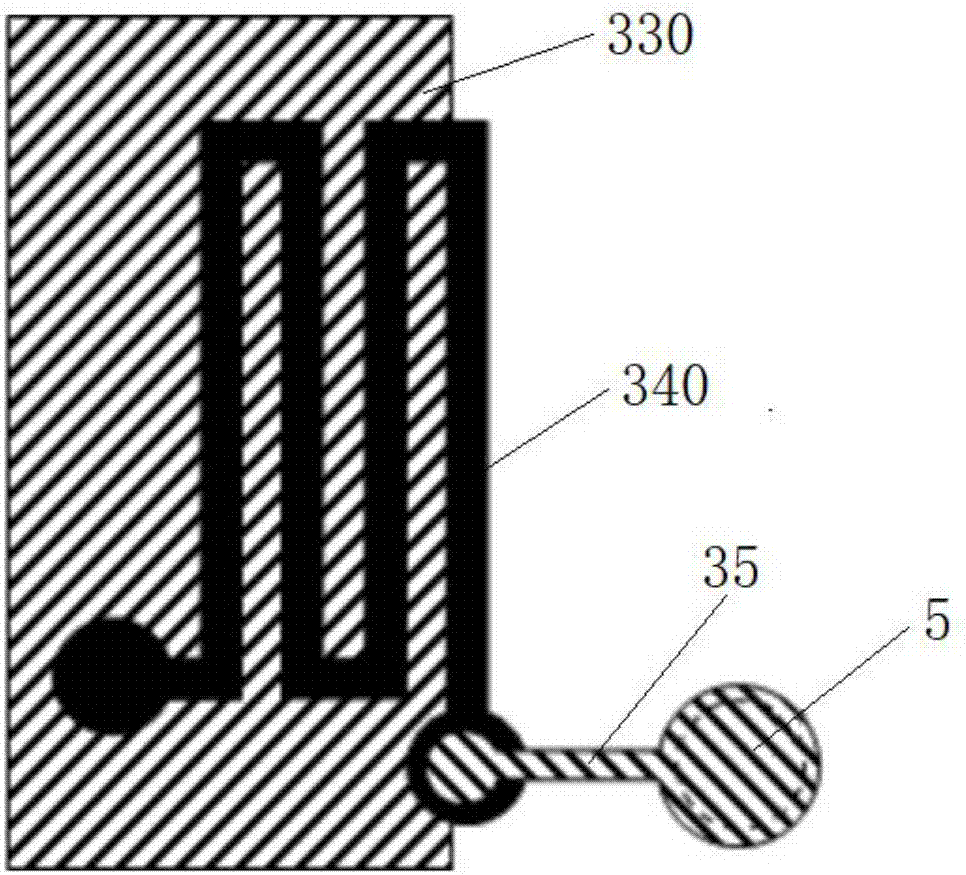
[0036] The embodiment of the present invention improves a chip package structure integrating passive components, such as figure 1 As shown, it includes: a package body 1 with a chip 2 packaged inside; the device surface of the chip 2 is located on the same plane as the first surface of the package body 1; the passive element layer 3 is arranged on the second surface of the package body 1; the first insulating Layer 4 is arranged on the passive element layer 3; the conductive column 5 is arranged in the package body 1, one end of the conductive column 5 is coupled with the passive element layer 3, and the other end is located on the same plane as the first surface of the package body 1; The wiring layer 6 is disposed on the first surface of the package body 1 and coupled with the chip 2 and the conductive pillar 5 . In this embodiment, the device surface of the chip 2 refers to the plane where the pads of the chip 2 are located, and the device surface of the chip 2 is located o...
Embodiment 2
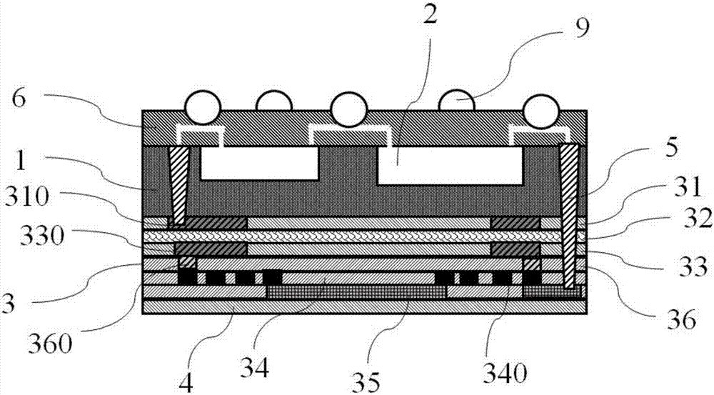
[0051] This embodiment provides a chip packaging method for integrating passive components, such as Figure 5 shown, including the following steps:
[0052] Step S1: providing a substrate, and forming an adhesive layer on the substrate. like Figure 6 As shown, in a specific embodiment, the material of the substrate 7 can be glass or ceramics, etc., and the material of the adhesive layer 8 can be thermal peeling adhesive or UV adhesive film, etc. In a specific embodiment, spray coating, spin coating or film sticking can be used and so on to form the adhesive layer 8 on the substrate 7 .
[0053] Step S2: Paste the device surface of the chip on the pasting layer. like Figure 7 As shown, in this embodiment, the device surface of the chip 2 refers to the plane where the pads of the chip 2 are located. In a specific embodiment, there may be one or more chips 2, and the number of chips 2 is determined according to the needs of actual application scenarios.
[0054] Step S3: ...
PUM
 Abstract
Description
Claims
Application Information
 - R&D Engineer
- R&D Manager
- IP Professional
- Industry Leading Data Capabilities
- Powerful AI technology
- Patent DNA Extraction
Browse by: Latest US Patents, China's latest patents, Technical Efficacy Thesaurus, Application Domain, Technology Topic, Popular Technical Reports.
© 2024 PatSnap. All rights reserved.Legal|Privacy policy|Modern Slavery Act Transparency Statement|Sitemap|About US| Contact US: help@patsnap.com