Fabrication method of chip
A manufacturing method and chip technology, applied in the direction of electrical components, circuits, semiconductor devices, etc., can solve the problems of poor growth thickness accuracy of epitaxial layers, large pressing stress growth stress, etc., to overcome the poor growth thickness accuracy, thickness Good accuracy and improved reliability
- Summary
- Abstract
- Description
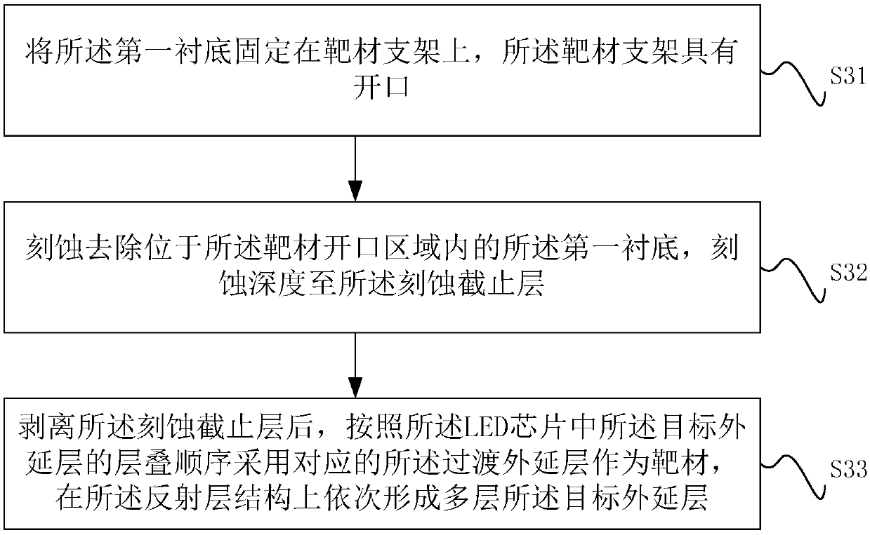
- Claims
- Application Information
AI Technical Summary
Problems solved by technology
Method used
Image


Examples
Embodiment Construction
[0047] The following will clearly and completely describe the technical solutions in the embodiments of the present invention with reference to the accompanying drawings in the embodiments of the present invention. Obviously, the described embodiments are only some, not all, embodiments of the present invention. Based on the embodiments of the present invention, all other embodiments obtained by persons of ordinary skill in the art without making creative efforts belong to the protection scope of the present invention.
[0048] In the prior art, when manufacturing LED chips, if a non-lattice-matched substrate is used to form the epitaxial layer of the LED chip, the lattice quality of the epitaxial layer will be poor, and the epitaxial stress will be larger and the thickness precision of the epitaxial layer will be lower. Poor, there is a large pressing stress during the substrate transfer process, these problems lead to poor reliability of the LED chip.
[0049] In order to so...
PUM
 Abstract
Description
Claims
Application Information
 - R&D
- Intellectual Property
- Life Sciences
- Materials
- Tech Scout
- Unparalleled Data Quality
- Higher Quality Content
- 60% Fewer Hallucinations
Browse by: Latest US Patents, China's latest patents, Technical Efficacy Thesaurus, Application Domain, Technology Topic, Popular Technical Reports.
© 2025 PatSnap. All rights reserved.Legal|Privacy policy|Modern Slavery Act Transparency Statement|Sitemap|About US| Contact US: help@patsnap.com