Evaluation apparatus and semiconductor device evaluation method
一种评价装置、半导体的技术,应用在单个半导体器件测试、半导体/固态器件制造、测量装置等方向,能够解决产生故障等问题,达到抑制局部放电、便利性高、抑制表面转印的效果
- Summary
- Abstract
- Description
- Claims
- Application Information
AI Technical Summary
Problems solved by technology
Method used
Image

Examples
Embodiment approach 1
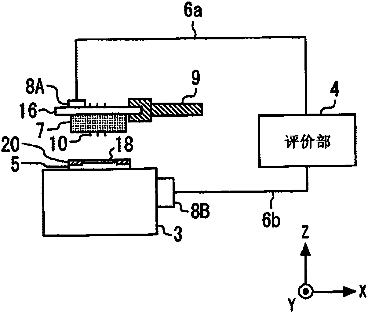
[0033] figure 1 It is a schematic configuration diagram of the evaluation device according to the first embodiment. The chuck table 3 is a base on which the semiconductor device 5 is vacuum-adsorbed. The holding means of the semiconductor device 5 is not limited to vacuum adsorption, but may be electrostatic adsorption or the like. exist figure 1 Although one semiconductor device 5 is shown in FIG. 1 , a plurality of semiconductor devices may be placed on the chuck table 3 . The surface of the chuck table 3 is electrically connected to the evaluation unit 4 via the connection portion 8B provided on the side surface of the chuck table and the signal line 6b attached to the connection portion 8B.
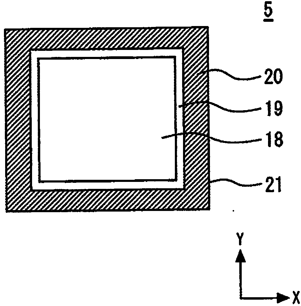
[0034] The semiconductor device 5 has a vertical structure in which a large current flows in the longitudinal direction of the semiconductor device 5 , that is, in the out-of-plane direction. Electrode pads 18 are formed on the upper surface of the semiconductor device 5 , and ele...
Embodiment approach 2
[0062] Figure 7 It is a bottom view of the insulator 7 etc. which concern on Embodiment 2. The insulating portions 64 , 68 are longer than the insulating portions 62 , 66 . Both ends of the insulating portions 62 and 66 are in contact with side surfaces in the longitudinal direction of the insulating portions 64 and 68 . The insulating part 62 has a lower surface 62a and a slope 62b, the insulating part 64 has a lower surface 64a and a slope 64b, the insulating part 66 has a lower surface 66a and a slope 66b, and the insulating part 68 has a lower surface 68a and a slope 68b. The lower surfaces 62a, 64a, 66a, 68a are thinner than the inclined surfaces 62b, 64b, 66b, 68b. In addition, similarly to Embodiment 1, insulating portions 62, 64, 66, and 68 each have a front end portion and a connection portion, and inclined surfaces 62b, 64b, 66b, and 68b and lower surfaces 62a, 64a, 66a, and 68a belong to the front end portion.
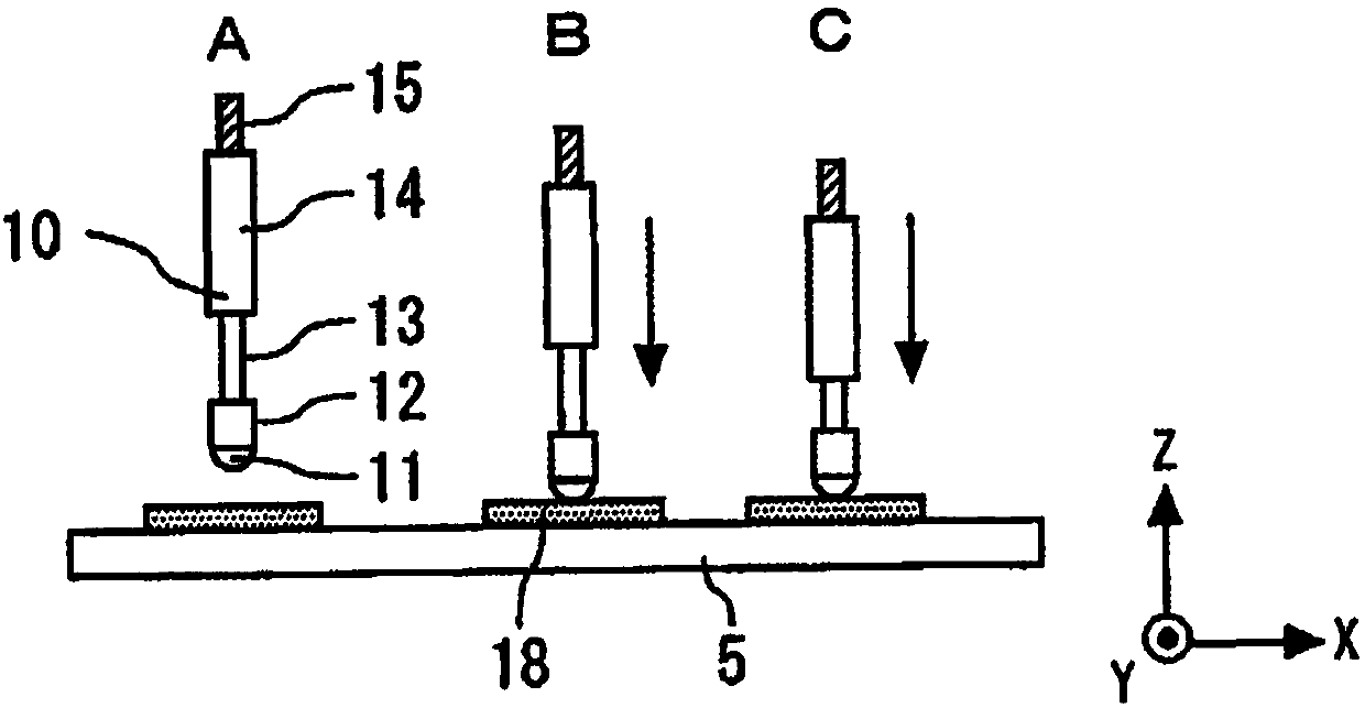
[0063] During the evaluation of the semiconductor ...
Embodiment approach 3
[0065] Figure 8 It is a sectional view of insulating parts 40 , 44 and the like according to the third embodiment. When a high voltage is applied to the probe 10 , it is preferable to increase the creeping distance on the high potential side near the probe 10 . Therefore, in Embodiment 3, the outer wall surfaces of the front end parts 23 and 25 are made into inclined surfaces 23d and 25d, so that the front end parts 23 and 25 have tapered shapes. Thus, the ratio of the lower surfaces 23c, 25c to Figure 5 The lower surfaces 23a, 25a are closer to the probe 10 side. In this case, the lower surface of the insulating portion is not in contact with the outermost peripheral portion of the terminal region 20 , but is in contact with the central portion of the terminal region 20 .
[0066] The insulating parts 42 and 46 also have the same shape as the insulating parts 40 and 44 of the present embodiment. Accordingly, the contact area between the insulator 7 and the terminal regi...
PUM
 Abstract
Description
Claims
Application Information
 - Generate Ideas
- Intellectual Property
- Life Sciences
- Materials
- Tech Scout
- Unparalleled Data Quality
- Higher Quality Content
- 60% Fewer Hallucinations
Browse by: Latest US Patents, China's latest patents, Technical Efficacy Thesaurus, Application Domain, Technology Topic, Popular Technical Reports.
© 2025 PatSnap. All rights reserved.Legal|Privacy policy|Modern Slavery Act Transparency Statement|Sitemap|About US| Contact US: help@patsnap.com